A fe-si-al system ternary amorphous thin film with adjustable bandgap width and preparation method thereof
An amorphous film and width technology, which is applied in the field of Fe-Si-Al ternary amorphous film and its preparation, can solve the problems of large film base mismatch, multi-phase mixing deterioration, stacking fault, twinning and other problems. Achieve the effect of avoiding lattice mismatch, avoiding multiphase mixing, and ensuring composition and performance
- Summary
- Abstract
- Description
- Claims
- Application Information
AI Technical Summary
Problems solved by technology
Method used
Image

Examples
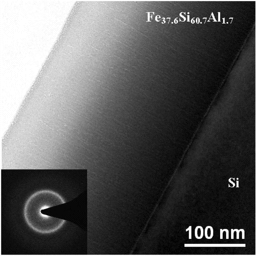
Embodiment 1
[0031] Example 1: Preparation of Fe by magnetron sputtering 37.6 Si 60.7 Al 1.7 film
[0032] (1) Preparation of alloy sputtering target, the steps are as follows:
[0033] 1. Preparation of materials: according to the atomic percentage of Fe and Al, it is respectively 4:0.15 to take by weighing each component value, and the purity of Fe and Al metal raw materials to be used: Fe is 99.99%, and Al is 99.999%;
[0034] ②Fe 4 Al 0.15 Smelting of alloy ingots: Put the metal mixture in the water-cooled copper crucible of the melting furnace, and use the vacuum arc melting method to smelt under the protection of argon gas. First, evacuate to 10 -2 Pa, and then filled with argon until the air pressure is 0.03±0.01MPa, and the control range of the melting current density is 150±10A / cm 2 , after melting, continue smelting for 10 seconds, cut off the power, let the alloy cool to room temperature with the copper crucible, then turn it over and place it in the water-cooled copper cr...
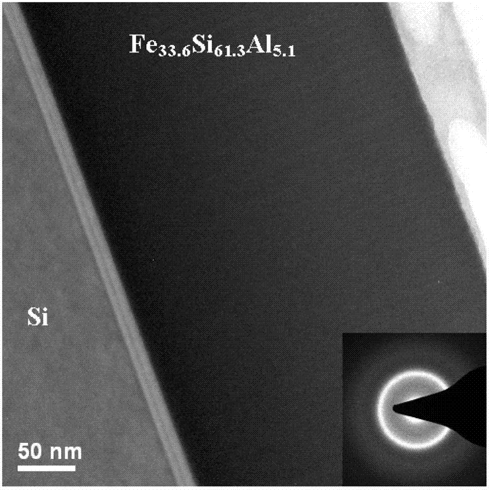
Embodiment 2
[0045] Example 2: Preparation of Fe by magnetron sputtering 33.6 Si 61.3 Al 5.1 film
[0046] The preparation process is the same as that of Example 1, only the Fe used to prepare the combined alloy sputtering target is adjusted. 4 Al z The number of alloy pieces and Z value: from 5.5 pieces of Fe 4 Al 0.5 Alloy flakes are made by pasting on the base Si target used for sputtering. The contents of Fe, Si, and Al in the EPMA films were 33.6 at.%, 61.3 at.%, and 5.1 at.%, respectively. The results of XRD and TEM showed that Fe 33.6 Si 61.3 Al 5.1 No crystal information was found in the sample, indicating that an amorphous film was prepared. The band gap width was measured to be 0.60 eV.
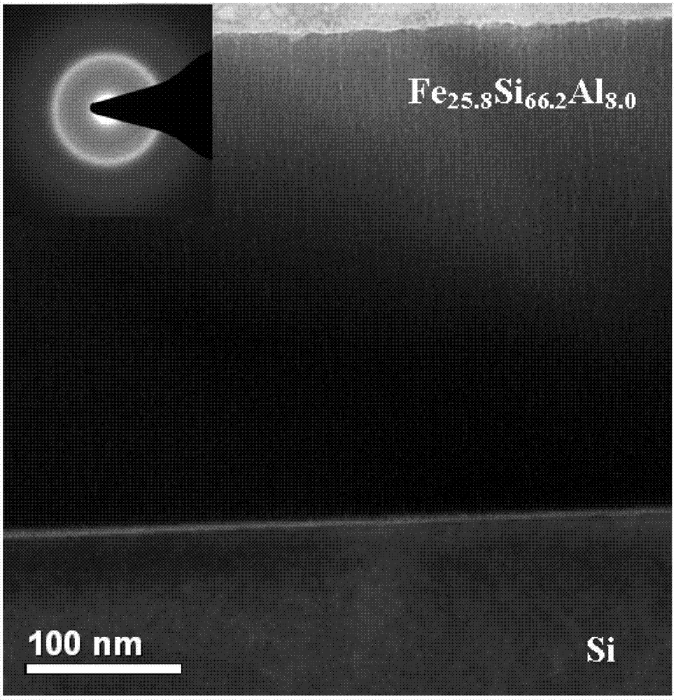
Embodiment 3
[0047] Example 3: Preparation of Fe by magnetron sputtering 25.8 Si 66.2 Al 8.0 film
[0048] The preparation process is the same as that of Example 1, only the Fe used to prepare the combined alloy sputtering target is adjusted. 4 Al z Number of alloy pieces and Z value: from 4 pieces of Fe 4 Al 1 Alloy flakes are made by pasting on the base Si target used for sputtering. The contents of Fe, Si, and Al in the EPMA films were 25.8 at.%, 66.2 at.%, and 8.0 at.%, respectively. The results of XRD and TEM showed that Fe 25.8 Si 66.2 Al 8.0 No crystal information was found in the sample, indicating that an amorphous film was prepared. The band gap width was measured to be 0.50 eV.
PUM
| Property | Measurement | Unit |
|---|---|---|
| thickness | aaaaa | aaaaa |
Abstract
Description
Claims
Application Information