

Radio frequency laterally diffused metal oxide semiconductor (LDMOS) component and manufacturing method thereof
A radio frequency and device technology, applied in the field of semiconductor integrated circuit manufacturing, can solve problems such as complex manufacturing process, and achieve the effects of reducing metal deposition, simple manufacturing process and improving breakdown voltage
- Summary
- Abstract
- Description
- Claims
- Application Information
AI Technical Summary
Problems solved by technology
Method used
Image

Examples
Embodiment Construction
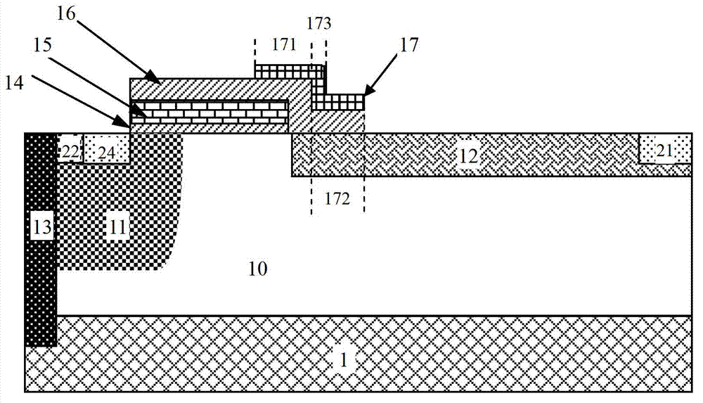
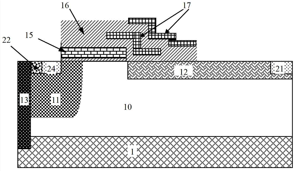
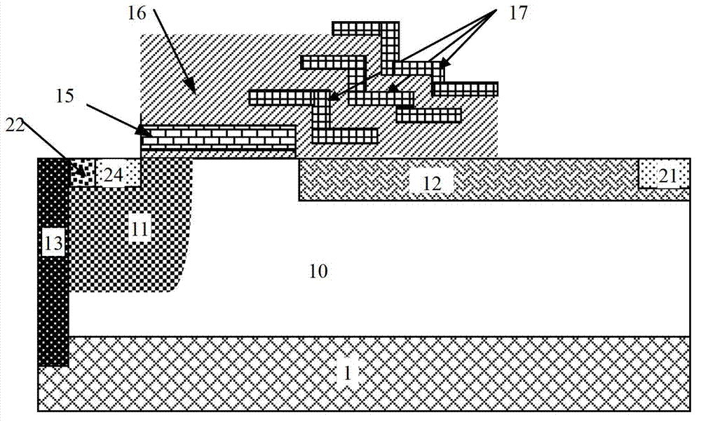
[0047] Such as Figure 4 It is a schematic diagram of an embodiment of the structure of the radio frequency LDMOS device of the present invention; the radio frequency LDMOS device of the embodiment of the present invention includes:
[0048] The P-type epitaxial layer 10 is formed on a semiconductor substrate such as a silicon substrate 1 .
[0049] The N-type drain end lightly doped drift region 12 is formed in the P-type epitaxial layer 10 .
[0050] A P well 11 is formed in the P-type epitaxial layer 10 , and there is a lateral distance between the P well 11 and the N-type drain end lightly doped drift region 12 .
[0051] A polysilicon gate 15 is formed above part of the P well 11 and is separated from the P well 11 by a gate oxide layer 14, and the part of the P well 11 covered by the polysilicon gate 15 is used to form a channel, The polysilicon gate 15 and the gate oxide layer 14 also extend to the P-type epitaxial layer 10 near the drain end and overlap with the N-ty...
PUM
| Property | Measurement | Unit |
|---|---|---|
| Width | aaaaa | aaaaa |
Abstract
Description
Claims
Application Information