
Processing method of field emitting cathode

A field emission cathode and processing method technology, applied in the field of FED, can solve the problems of film damage, unsatisfactory field emission performance, affecting the field emission performance of CNTs film, etc., and achieve the effect of increasing the emission current and reducing the field strength.

Inactive Publication Date: 2013-04-17
QINGDAO SHENGJIA INFORMATION TECH
View PDF5 Cites 3 Cited by
  • Summary
  • Abstract
  • Description
  • Claims
  • Application Information

AI Technical Summary

Problems solved by technology

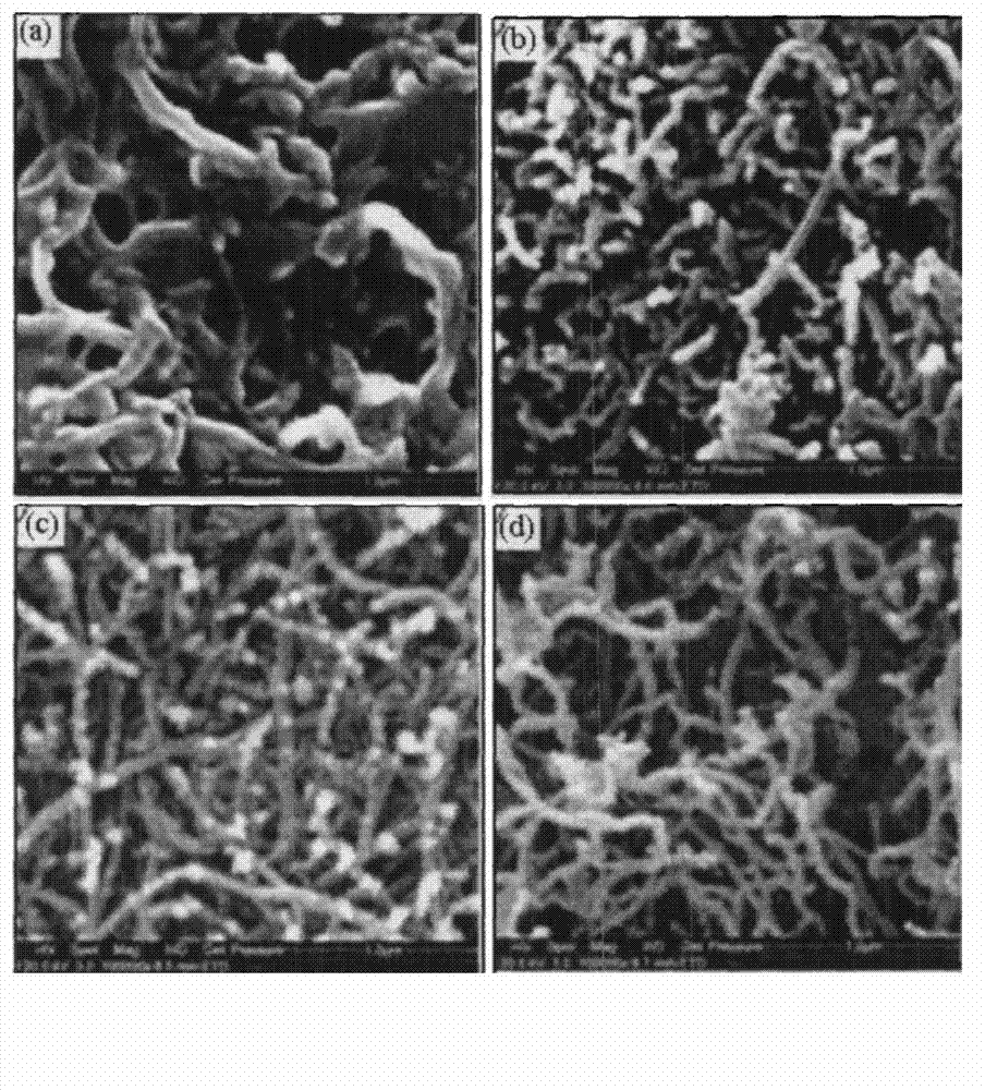
However, the produced CNTs are entangled with each other, the surface is surrounded by pulping materials, and the tips are not protruding. The residual organic matter after sintering still seriously affects the field emission performance of the CNTs film.
In order to solve these problems, people have tried methods such as plasma bombardment, ion beam irradiation, tape sticking], mechanical friction and soft rubber roller rolling to process the screen-printed FED cathode, but because the film is damaged, or it is not easy to accurately control The improvement of field emission performance is also limited due to problems such as processing process and effect
[0004] The method of preparing carbon tube thin film FED cathode by screen printing method (or coating method) has good practical application prospects, but the field emission performance is not satisfactory (mainly in terms of turn-on voltage, emission current and emission stability, etc.)

Method used


Image

  • Processing method of field emitting cathode
  • Processing method of field emitting cathode

Examples


Embodiment Construction

[0015] (l) Preparation of MWCNTs thin film

[0016] The MWCNTs used in the present invention are prepared by chemical vapor deposition (CVD). The diameter is 20~40nm, and the length is about 5μm. The purified MWCNT powder was dispersed in anhydrous ethanol by ultrasonic waves, dried naturally at room temperature and fully ground, then mixed with an organic vehicle and stirred for 1-2 hours as a cathode slurry. Print a layer of silver paste film electrodes with an area of ​​60mm×25mm on the glass substrate. After the sintering treatment, the prepared carbon tube slurry is used to print the carbon tube film on the center of the substrate with a 200-mesh screen. All the samples were put together in a tube furnace and sintered under Ar environment before use.

[0017] (2) Laser ablation treatment

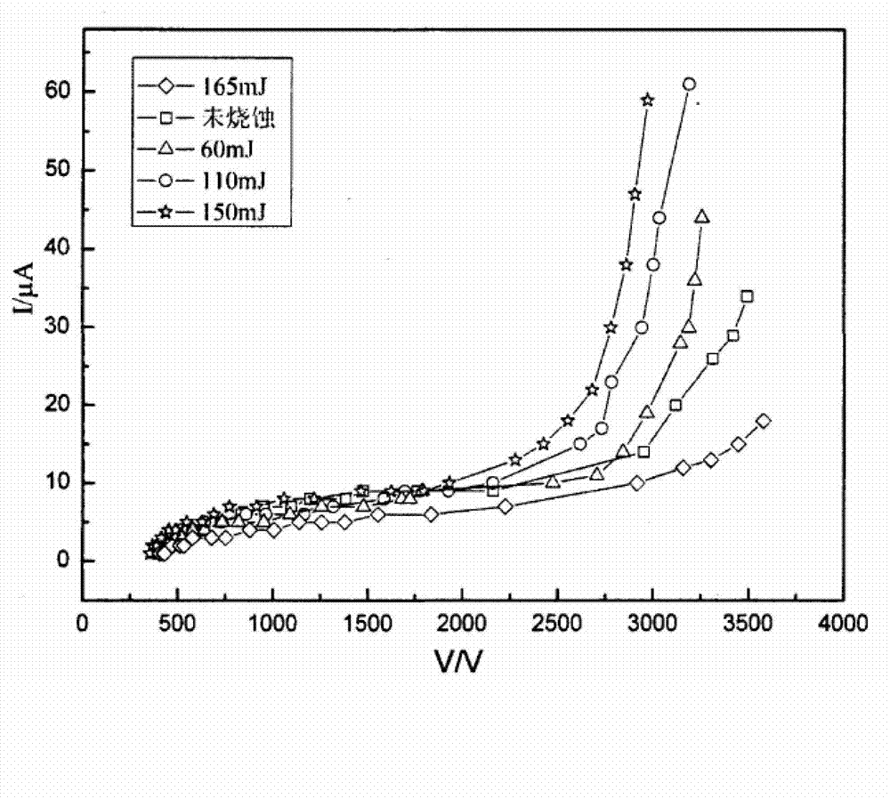
[0018] A Lambda Physik comPex102 KrF excimer laser system was used in this experiment. The output wavelength of the laser is 248nm, and the pulse width is 30ns. The laser has a la...


PUM

PropertyMeasurementUnit
diameteraaaaaaaaaa
lengthaaaaaaaaaa

Abstract

The invention provides a processing method of a field emitting cathode. The processing method of the field emitting cathode comprises the following steps of: preparing an MWCNT (Multi Walled Carbon Nano-Tube) by using a chemical vapor deposition method; ultrasonically diffusing purified MWCNT powder in absolute ethyl alcohol, naturally drying at a room temperature and sufficiently grinding, and mixing with an organic carrier and using as cathode slurry after stirring for 1-2 hours; printing a layer of silver slurry thin film electrode with an area of 60 mm*25 mm on a glass substrate; printing a carbon tube thin film at the center of the substrate by the prepared carbon tube slurry through a 200-mesh silk screen after sintering; putting all samples in a tube type furnace together, and sintering at the presence of Ar; and carrying out laser ablation treatment for 5 minutes in air by using an excimer laser system. Therefore, the switch-on field intensity is reduced, and the emitting current is increased.

Description

technical field [0001] The invention belongs to the field of FED, in particular to a method for modifying the surface of a screen-printed multi-walled carbon nanotube (MWCNTs) film. Background technique [0002] The main difficulties faced by FED display devices, in addition to problems such as vacuum packaging, all come from the cathode manufacturing process. The difficulties of controlling the uniformity and stability of field emission and reducing the cost of the driving circuit are directly restricted by the material and structure of the FED cathode. Spindt-type devices require the fabrication of hundreds or thousands of cathode arrays of "sharp cones and round holes" within a pixel size range. This makes the photolithography process and thin film preparation very complicated, and the production cost is also very expensive. Difficulties in the manufacturing process of the cathode also lead to poor uniformity of the shape of the cone array and unsatisfactory overall sta...

Claims


Application Information

Patent Timeline
Patent Type & Authority Applications(China)
IPC IPC(8): H01J9/02
Inventor 于正友肖太升刘雷
Owner QINGDAO SHENGJIA INFORMATION TECH
Learn More