Manufacturing method of oxide thin film transistor

A technology of oxide film and manufacturing method, applied in semiconductor/solid-state device manufacturing, electrical components, circuits, etc., to achieve the effect of reducing process difficulty, avoiding current crowding, and reducing process temperature

Active Publication Date: 2015-10-21
SHENZHEN DANBANG INVESTMENT GROUP
View PDF4 Cites 2 Cited by
  • Summary
  • Abstract
  • Description
  • Claims
  • Application Information

AI Technical Summary

Problems solved by technology

[0004] In order to solve the above technical problems, so that the field effect mobility of the transistor is higher, and the current crowding phenomenon is not easy to occur when the thin film field effect transistor is at a low drain voltage, the invention provides a manufacturing method of an oxide thin film transistor

Method used


Image

  • Manufacturing method of oxide thin film transistor
  • Manufacturing method of oxide thin film transistor
  • Manufacturing method of oxide thin film transistor

Examples


no. 1 example

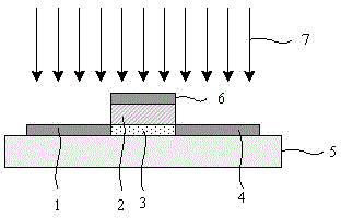
[0028] refer to figure 1 and 2 A partial structure of a coplanar oxide thin film transistor includes a substrate 5, an oxide semiconductor layer, a gate insulating layer 2 and a gate 6, and an oxide semiconductor layer is formed on the surface of the substrate 5, and the oxide semiconductor layer includes The channel region 3 opposite to the gate 6, and the first contact region 1 (for contacting the source 8 ) and the second contact region 4 (for contacting the drain 9 ) on both sides of the channel region 3 contact region), the channel region 3 is located between the first contact region 1 and the second contact region 4 , a gate insulating layer 2 is formed on the oxide semiconductor layer, and a gate 6 is formed on the gate insulating layer 2 .

[0029] The manufacturing method of the coplanar oxide thin film transistor of this embodiment includes the following steps:

[0030] (1) Reference figure 1 , deposit an oxide semiconductor thin film on glass, quartz, silicon waf...

no. 2 example

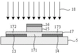
[0046] Such as image 3 As shown, a schematic cross-sectional view of a top-gate thin film transistor, the thin film transistor includes a substrate 5, a source 13 and a drain 14 formed on the substrate 5, an oxide semiconductor layer 17 formed on the source 13 and the drain 14 , the gate insulating layer 15 formed on the oxide semiconductor layer 17, the gate 16 formed on the gate insulating layer 15, the oxide semiconductor layer 17 includes a channel region 171 opposite to the gate 16, and the The first contact region 172 (in contact with the source 13) and the second contact region 173 (in contact with the drain 14) on both sides of the channel region 171, the channel region 171 is located between the source 13 and the drain 14; wherein the gate 16 Self-alignment can be formed with the gate insulating layer 15 and the channel region 171 .

[0047] Such as Figure 4 As shown, another top gate oxide thin film transistor structure, the thin film transistor includes a substr...

no. 3 example

[0057] refer to Figure 6 It is a schematic cross-sectional view of a bottom-gate thin film transistor according to the third embodiment. The thin film transistor includes a substrate 5, a gate 30 formed on the substrate 5, a gate insulating layer 32 formed on the gate, and a gate insulating layer 32 formed on the gate insulating layer. 32, an etching stopper layer 33 formed on the oxide semiconductor layer 31, source and drain electrodes 34 and 35 formed on the oxide semiconductor layer 31, the oxide semiconductor layer includes A standard channel region 311 , a first contact region 312 (contacting to the source 34 ) and a second contact region 313 (contacting to the drain 35 ) respectively located on both sides of the channel region 311 .

[0058] The manufacturing method of the bottom gate oxide thin film transistor of this embodiment includes the following steps.

[0059] (1) Reference Figure 6, form a grid conductive layer on glass, quartz, silicon wafer or other flexi...


PUM


Abstract

The invention discloses a manufacturing method of an oxide thin film transistor. The oxide thin film transistor comprises an oxide semiconductor layer, a source electrode and a drain electrode. The oxide semiconductor layer comprises a channel region, and a first contact region and a second contact region on both sides of the channel region respectively. The source electrode is contacted with the first contact region and the drain electrode is contacted with the second contact region. The oxide semiconductor layer adopts indium oxide, gallium oxide, zinc oxide or tin oxide, or binary or multibasic oxides of indium, gallium, zinc, and tin. The first and second contact regions are radiated by electron beams. According to the manufacturing method provided by the invention, the field effect migration rate of the oxide thin film transistor is improved, and meanwhile the current crowding phenomenon is reduced or avoided; in addition, the process temperature is effectively reduced, and a substrate is maintained in a low temperature state, therefore, a flexible substrate can be used. The processing difficulty can be reduced, and the production cost can be lowered.

Description

【Technical field】 [0001] The invention relates to the field of transistors, in particular to a method for manufacturing an oxide thin film transistor. 【Background technique】 [0002] Compared with the amorphous silicon TFT (thin film field effect transistor) widely used in the active drive matrix of liquid crystal display, the oxide semiconductor TFT has the following advantages: (1) high field effect mobility; (2) high switching ratio; (3) The temperature of the preparation process is low; (4) Large-area amorphous films can be produced, with good uniformity and good and consistent electrical properties; (5) Less affected by visible light, more stable than amorphous silicon and organic thin film transistors; (6) ) can be made into transparent devices. In the field of flat panel display, oxide TFT technology almost meets all the requirements of many display modes including AMOLED drive, fast ultra-large-screen liquid crystal display, 3D display and so on. In terms of flexib...

Claims


Application Information

Patent Timeline
Patent Type & Authority Patents(China)
IPC IPC(8): H01L21/34H01L21/44H01L21/428
Inventor 刘萍
Owner SHENZHEN DANBANG INVESTMENT GROUP
Why Eureka
Try Eureka