Preparation method of back passivated battery

A technology of back passivation and batteries, which is applied in the manufacture of circuits, electrical components, final products, etc., can solve the problems of complex technology and high energy consumption, and achieve the effects of good spectral response, improved utilization rate, and good electrical passivation effect

Active Publication Date: 2013-04-17
山东一开电气设备有限公司
View PDF4 Cites 9 Cited by
  • Summary
  • Abstract
  • Description
  • Claims
  • Application Information

AI Technical Summary

Problems solved by technology

[0004] At present, the existing back passivation battery preparation method mainly adopts two-ste

Method used


Image

  • Preparation method of back passivated battery
  • Preparation method of back passivated battery

Examples


Embodiment 1

[0025] The operation steps are as follows:

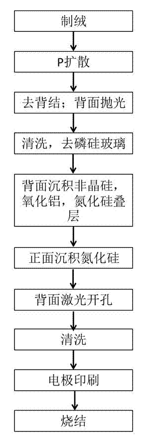
[0026] Select a P-type monocrystalline silicon wafer with a crystal plane of (100) and a doping concentration of 2 Ω·cm, perform routine cleaning, and prepare a surface texture in a 1.5% KOH solution at a temperature of 70°C for 20 minutes.

[0027] Put the textured silicon wafer into the P diffusion tube for diffusion, the diffusion temperature is 830°C, and the diffusion square resistance is 60Ω / cm.

[0028] Etch and polish the backside of the silicon wafer in 20% KOH solution at a temperature of 70°C for 5 minutes.

[0029] with the main component being H 2 o 2 and NH 3 .H 2 The mixed solution of O was used to clean the back of the silicon wafer for 15 minutes, and the front and back of the silicon wafer were cleaned with 5% HF solution for 5 minutes.

[0030] A laminated passivation film of amorphous silicon, aluminum oxide and silicon nitride is deposited on the back of the silicon wafer by PECVD with a thickness of 83nm. ...

Embodiment 2

[0037] The operation steps are as follows:

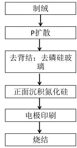
[0038] Select a P-type monocrystalline silicon wafer with a crystal plane of (100) and a doping concentration of 1 Ω·cm, perform routine cleaning, and prepare a suede surface in a 1% KOH solution at a temperature of 70°C for 24 minutes.

[0039] Put the textured silicon wafer into the P diffusion tube for diffusion, the diffusion temperature is 880°C, and the diffusion square resistance is 65Ω / cm.

[0040] Etch and polish the backside of the silicon wafer in 15% KOH solution at a temperature of 74°C for 5 minutes.

[0041] with the main component being H 2 o 2 and NH 3 .H 2 Clean the back of the silicon wafer with a mixed solution of O for 20 minutes, and clean the front and back of the silicon wafer with 10% HF solution for 3 minutes.

[0042] Deposit amorphous silicon, aluminum oxide and silicon nitride lamination passivation film with a thickness of 75nm on the back of the silicon wafer by PECVD.

[0043] A silicon nitride ...


PUM

PropertyMeasurementUnit
Thicknessaaaaaaaaaa
Thicknessaaaaaaaaaa
Thicknessaaaaaaaaaa

Abstract

The invention relates to a preparation method of a back passivated battery, and belongs to the technical field of a production method of a solar battery. The process comprises the steps of: first, cleaning a P type monocrystalline silicon wafer and making a texture surface, and then carrying out P diffusion; then, corroding and polishing the back of the silicon wafer by an etchant solution; then, respectively cleaning the front face of the silicon wafer by HF solution, and cleaning the back of the silicon wafer by an RCA method; then, sequentially depositing amorphous silicon, aluminum oxide and silicon nitride on the back of the battery, and depositing silicon nitride on the front face of the silicon wafer; removing deposited thin film layer locally on the back of the silicon wafer by laser or corrosive slurry; and finally printing an electrode and sintering the electrode. The preparation method has the beneficial effects that the battery piece is laminated and passivated on the back, in particular by amorphous silicon, aluminum oxide and silicon nitride, so that the back of the battery not only has a good electric passivating effect, but also has a good internal reflective effect to a long-wave band. The long-wave band of the battery has a good spectral response, so that the utilization rate of sunlight and the photoelectric conversion efficiency of the battery are improved.

Description

technical field [0001] The invention relates to a novel back passivation battery method and belongs to the technical field of solar battery production methods. Background technique [0002] Photovoltaic power generation technology is an important new energy technology field in the 21st century, but the efficiency of photovoltaic power generation in production is relatively low. It is an urgent task to seek new technologies, new materials, and new processes to improve the photoelectric conversion efficiency of solar cells and reduce unit power generation costs. [0003] The photoelectric conversion efficiency of a solar cell is closely related to the photoelectric response of the cell to each band of solar incident light. Existing conventional solar cells have a good response in the visible light band, but due to the strong recombination effect on the back of the battery, the long-wave band in sunlight is rarely used. [0004] At present, the existing back passivation batte...

Claims


Application Information

Patent Timeline
IPC IPC(8): H01L31/18
CPCY02P70/50
Inventor 刘亚郭志球苏旭平王建华涂浩彭浩平吴长军
Owner 山东一开电气设备有限公司
Why Eureka
Try Eureka