Graphene capacitive touch screen metal electrode fine patterning method

A capacitive touch screen, metal electrode technology, applied in metal material coating process, superimposed layer plating, electrical digital data processing and other directions, can solve the problem that the mask alignment accuracy and speed cannot meet the needs of normal production, reduce production Efficiency and product yield, low film conductivity and transparency

Inactive Publication Date: 2013-04-24
无锡力合光电石墨烯应用研发中心有限公司 +1
View PDF4 Cites 25 Cited by
  • Summary
  • Abstract
  • Description
  • Claims
  • Application Information

AI Technical Summary

Problems solved by technology

Although the ITO film produced by the existing process has high conductivity and transparency, which can basically meet the needs of some electronic products for these two technical indicators, there are still many difficulties that are difficult to overcome:
[0005] (1) ITO is very brittle and brittle, so it is easy to be worn during application or cracks and falls off during bending, which affects the service life
[0006] (2) After the ITO film is formed, high temperature treatment is required to achieve high conductivity. When using a plastic substrate, due to the limited processing temperature, the conductivity and transparency of the film are low
[0007] (3) Affected by raw mat

Method used


Image

  • Graphene capacitive touch screen metal electrode fine patterning method
  • Graphene capacitive touch screen metal electrode fine patterning method
  • Graphene capacitive touch screen metal electrode fine patterning method

Examples


Embodiment 1

[0095] A fine patterning method for graphene capacitive touch screen metal electrodes, comprising the steps of:

[0096] (1) Prepare a single layer or 2~3 atomic layer graphene film on a glass substrate by CVD transfer method; CVD transfer method refers to the formation of 0.3~ 1.5nm thick graphene film, and then the graphene film layer is transferred to the substrate by chemical transfer method;

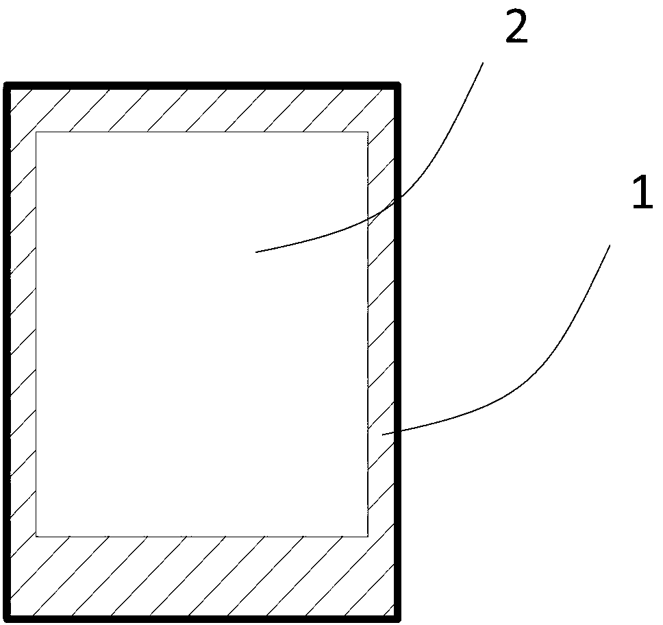
[0097] (2) Use the spin coating method to uniformly cover the positive photoresist on the graphene layer, combine with a suitable mask plate, and expose the lead electrode area (1) and the window touch area (2) through exposure and development;

[0098] (3) Deposit the lead metal layer on the graphene substrate by magnetron sputtering method, and the film thickness can be 200~1000nm;

[0099] (4) Using online roller brushing or manual wiping, the positive glue remover composed of ethanolamine and dimethyl sulfoxide removes the photosensitive glue / metal film layer, temperature contr...

Embodiment 2

[0102] A fine patterning method for graphene capacitive touch screen metal electrodes, comprising the steps of:

[0103] (1) Using the method disclosed in CN102220566A to prepare a graphene film, specifically: placing the copper foil substrate in a vacuum tube furnace, injecting hydrogen into the vacuum chamber while removing oxygen in the vacuum chamber, and raising the temperature to 1000°C , and then methane gas is injected into the vacuum chamber to obtain a metal substrate deposited with graphene; the thickness of the graphene film is 0.3nm;

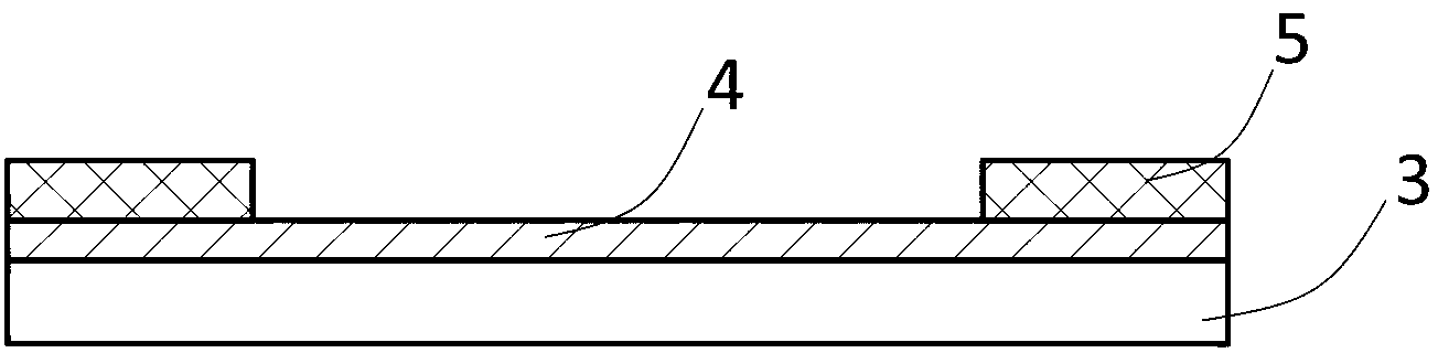
[0104] Then through the method of chemical transfer, using PDMS as the medium, the graphene film layer is transferred onto the substrate, and the whole board is obtained as the substrate I of the layered structure of graphene / substrate; the structure of the substrate I is as follows image 3 shown ( image 3 is a structural schematic diagram of the substrate 1 described in an embodiment of the present invention);

[0105] (2) Coat...

Embodiment 3

[0112] A fine patterning method for graphene capacitive touch screen metal electrodes, comprising the steps of:

[0113] (1) Using the method disclosed in CN102220566A to prepare a graphene film, specifically: placing the copper foil substrate in a vacuum tube furnace, injecting hydrogen into the vacuum chamber while removing oxygen in the vacuum chamber, and raising the temperature to 1000°C , and then methane gas is injected into the vacuum chamber to obtain a metal substrate deposited with graphene; the thickness of the graphene film is 1nm;

[0114]Then through the method of chemical transfer, with PMMA as the medium, the graphene thin film is transferred onto the glass substrate, and the graphene film layer is transferred onto the substrate to obtain the substrate I with a layered structure of graphene / substrate. ;

[0115] (2) Coating the positive photoresist evenly on the graphene layer of the substrate I to obtain the substrate II with a layered structure of photoresi...


PUM

PropertyMeasurementUnit
Thicknessaaaaaaaaaa
Thicknessaaaaaaaaaa
Thicknessaaaaaaaaaa

Abstract

The invention relates to a graphene capacitive touch screen metal electrode fine patterning method. The method aims at a substrate transferred with graphene, and during metal film layer deposition, photo-sensitive resist is used for protecting a window touch area of a touch screen, and the touch screen is subjected to complete patterning finally after photo-sensitive resist removal. The method is beneficial to industrialized large-scale production and processing of patterned metal electrode film layers and low in equipment transformation cost, etching speed of metal electrode layers and graphene layers is increased, a yellow light fine-etching process is avoided, manufacture procedures can be simplified greatly, cost is saved, and product yield is increased.

Description

technical field [0001] The invention relates to a fine patterning method of a metal electrode of a graphene capacitive touch screen, in particular to a method for manufacturing a metal electrode film layer with a fine pattern design that can be applied on a graphene material of a capacitive touch screen. Background technique [0002] The touch screen is an input device that can facilitate the interaction between people and computers and other portable mobile devices. In recent years, capacitive touch screens based on transparent conductive films have been widely used in mobile Internet devices, such as smartphones and portable tablet computers. The touch screen is divided into window touch area 2 and lead electrode area 1 according to the functional area. The lead electrode area 1 is connected to the external structure through the controller ( figure 1 It is a schematic diagram of the functional area of ​​the capacitive touch screen). [0003] The currently popular capacit...

Claims


Application Information

Patent Timeline
IPC IPC(8): G06F3/044G02F1/133C23C28/00
Inventor 刘志斌赵斌黄海东陈凯
Owner 无锡力合光电石墨烯应用研发中心有限公司
Why Eureka
Try Eureka