Fan-out Panel Level ball grid array (BGA) package part manufacture process

A manufacturing process and packaging technology, which is used in semiconductor/solid-state device manufacturing, electrical components, electrical solid-state devices, etc. The number of pins, better performance requirements, and high packaging costs can shorten the current and signal transmission distance, reduce warpage, improve electrical performance and product reliability.

Inactive Publication Date: 2013-05-08
HUATIAN TECH XIAN
View PDF4 Cites 6 Cited by
  • Summary
  • Abstract
  • Description
  • Claims
  • Application Information

AI Technical Summary

Problems solved by technology

[0003]The traditional QFN packaging technology requires the use of lead frames and bonding wires. To a certain extent, not only the packaging cost is high, but also the packaging thickness is relatively large, which cannot meet the needs of many electronic products. Pin, high density, small and thin requirements
[0004] Compared with the traditional packaging technology, Fan-in Panel BGA packaging technology reduces the thickness of the package to a certain extent and reduces the cost, but the distance between balls and I / Due to the limitation of chip size, the O number cannot meet the higher pin count and better performance requirements of packaged products

Method used


Image

  • Fan-out Panel Level ball grid array (BGA) package part manufacture process
  • Fan-out Panel Level ball grid array (BGA) package part manufacture process
  • Fan-out Panel Level ball grid array (BGA) package part manufacture process

Examples


Embodiment Construction

[0021] The present invention will be described in further detail below in conjunction with the accompanying drawings.

[0022] As shown in the figure: A manufacturing process of Fan-out Panel Level BGA package, which is carried out according to the following steps:

[0023] The first step, wafer thinning: use the anti-fragmentation process to thin the wafer to the specified thickness;

[0024] The second step, wafer dicing: the wafer with a thickness of 150 μm or more adopts the ordinary dicing process, and the wafer with a thickness of less than 150 μm adopts a double-knife dicing machine and its process;

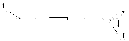
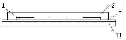
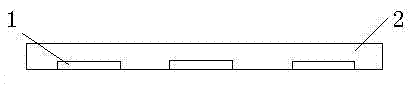
[0025] The third step, flipping the core: before flipping the core, adhere the double-sided adhesive film 7 to the high temperature resistant glass 11 with a smooth and flat surface, wherein the thickness of the double-sided adhesive film 7 should not be large. It must be less than 3um, and the front of the film needs to mark the position of the core in advance, set up an...


PUM


Abstract

The invention discloses a Fan-out Panel Level ball grid array (BGA) package part manufacture process. The manufacture process comprises the following steps of thinning a wafer, scratching a wafer, reversely bonding a chip, plastically packing, tearing a film, turning, carrying out primary insulation treatment, punching holes, distributing copper wires, carrying out secondary insulation treatment, punching holes, plating nickel porpezite, printing, reflow soldering and cutting. Compared with traditional package technique, the manufacture process saves cost, can achieve multi-pin, high-density, small and thin package and has the advantages of being good in radiation, electric performance and coplanarity and the like.

Description

technical field [0001] The invention relates to a manufacturing process of a Fan-out Panel Level BGA package, belonging to the technical field of semiconductor packaging. Background technique [0002] Today's electronic packaging must not only provide protection for the chip, but also meet the ever-increasing requirements for performance, reliability, heat dissipation, and power distribution at a certain cost. The increase in the speed and processing capacity of functional chips requires more pins , faster clock frequency and better power distribution. The market needs electronic products to have more functions, longer battery life and smaller geometric size, adapt to lead-free soldering (protect the environment) and effectively reduce costs. [0003] The traditional QFN packaging technology requires the use of lead frames and bonding wires. To a certain extent, not only the packaging cost is high, but also the packaging thickness is relatively large, which cannot meet the ...

Claims


Application Information

Patent Timeline
Patent Type & Authority Applications(China)
IPC IPC(8): H01L21/50H01L21/60
CPCH01L24/19H01L2224/12105H01L2224/19H01L2924/00012
Inventor 朱文辉王虎谌世广刘卫东谢建友
Owner HUATIAN TECH XIAN
Why Eureka
Try Eureka