Microwell plate chemical copper activating back scrubbing process and system thereof

A technology of chemical copper and micro-orifice plate, applied in the direction of electrical connection formation of printed components, etc., can solve the problems of poor backlight of PCB board, unfavorable nickel sinking, long production cycle, etc., to reduce the risk of bad backlight, reduce the concentration of activator, The effect of reducing labor intensity

Active Publication Date: 2013-05-15
金悦通电子(翁源)有限公司
View PDF1 Cites 9 Cited by
  • Summary
  • Abstract
  • Description
  • Claims
  • Application Information

AI Technical Summary

Problems solved by technology

This process is complicated, the production cycle is long, and the cost is high. After activation, the activated target in the PCB hole is easily dissolved in the subsequent secondary countercurrent rinsing and washing, which leads to the problem of poor backlight on the PCB and reduces the The product yield of the PCB board, in order to prevent the activation target from being dissolved, the concentration of the activator can be increased, and the increase of the concentration of the activator will increase the cost of the enterprise
[0004] Chinese patent discloses an application number: 201210332993.3, a method for setting a metal target layer in the conductive layer of a printed circuit board and its layered structure, the steps of which are: first coat the insulating substrate with copper, and then bake the board, After that, the drillin

Method used


Image

  • Microwell plate chemical copper activating back scrubbing process and system thereof
  • Microwell plate chemical copper activating back scrubbing process and system thereof
  • Microwell plate chemical copper activating back scrubbing process and system thereof

Examples


Embodiment Construction

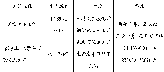
[0039] The embodiment of the present invention optimizes the original copper sinking process, so that the activated PCB board is pre-soaked again, which reduces the risk of bad backlight, improves the quality of the produced board product, greatly improves the work efficiency, and reduces the Labor intensity, and at the same time, because the activation target in the hole is not easy to dissolve, the concentration of the activator in the activation cylinder can be reduced, and the production cost is reduced.

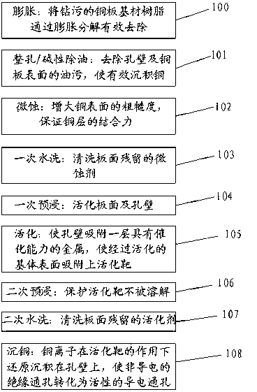
[0040] see figure 1 , which is a schematic flow chart of a microporous plate chemical copper activation backwashing process provided by the present invention.

[0041] A microporous plate chemical copper activation backwashing process provided in this embodiment includes:

[0042] Step 100, expansion: effectively remove the drilled copper substrate resin through expansion and decomposition;

[0043] Step 101, whole hole / alkaline degreasing: remove the oil on the wall o...


PUM

PropertyMeasurementUnit
Proportionaaaaaaaaaa

Abstract

The invention provides a microwell plate chemical copper activating back scrubbing process and a system of the microwell plate chemical copper activating back scrubbing process. The process includes the steps of microetching, first time wash, first time preimpregnation, activation, second time wash, copper deposition and second time preimpregnation. The microetching is used for increasing roughness of the surface of copper and ensuring combining force of a copper layer. The first time wash is used for washing remaining micro corrosion agent of a panel. The first time preimpregnation is used for activating the panel and hole wall. The activation is used for enabling the hole wall to adsorb a layer of metal which has catalytic ability and enabling the surface of the matrix to attach to a activation target. The second wash is used for washing remaining activation agent of the panel. The copper deposition is used for enabling non-conductive insulation hole to be transformed into an active conductive through hole under the action of copper ions in the activation of target reduction deposition on the hole wall. The second time preimpregnation is used for ensuring that the activation target is not solved. Due to the fact that the microwell plate chemical copper activating back scrubbing process and the system of the microwell plate chemical copper activating back scrubbing process are conducted, the activation target in a printed circuit board (PCB) is not solved, the risk of poor backlight is reduced, quality of products is improved, and production cost is reduced.

Description

technical field [0001] The invention relates to the technical field of PCB boards, in particular to a microporous plate chemical copper activation backwashing process and a system thereof. Background technique [0002] PCB (Printed Circuit Board), the Chinese name is printed circuit board, referred to as printed board, is one of the important components of the electronics industry. Almost every kind of electronic equipment, ranging from electronic watches and calculators to computers, communication electronic equipment, and military weapon systems, as long as there are electronic components such as integrated circuits, printed boards are used for the electrical interconnection between them. . [0003] In the production and processing of PCB boards with through holes, a key link is the hole metallization process. This process converts non-conductive insulating through-holes into active conductive through-holes, and the existing PCB boards make holes for conduction. The most...

Claims


Application Information

Patent Timeline
IPC IPC(8): H05K3/42
Inventor 胡俊
Owner 金悦通电子(翁源)有限公司
Why Eureka
Try Eureka