Phosphorous gettering method of metallurgy polycrystalline silicon wafer, silicon wafer and solar cell prepared by silicon wafer

A polysilicon wafer and phosphorus gettering technology, which is applied in the manufacture of circuits, electrical components, and final products, can solve the problems of long battery production cycle, new dislocations in silicon wafers, and small phosphorus diffusion coefficient, so as to improve the photovoltaic Effects of conversion efficiency, improved lifetime, and shortened diffusion time

Inactive Publication Date: 2013-05-22
INNER MONGOLIA RIYUE SOLAR ENERGY TECH
View PDF7 Cites 10 Cited by
  • Summary
  • Abstract
  • Description
  • Claims
  • Application Information

AI Technical Summary

Problems solved by technology

However, the diffusion coefficient of phosphorus in silicon is very small, and usually requires a higher diffusion temperature and a longer diffusion time to achieve the gettering effect.
Conventional phosphorus gettering methods generally use high-temperature diffusion (≥1000°C) to achieve better gettering effects, but high temperatures will cause new dislocations and other defects in silicon wafers; while medium-temperature diffusion (≤900°C) requires more A long time, generally more than 2 hours, makes the production cycle of the cell long, increases energy consumption, and is not suitable for industrialization

Method used


Image

  • Phosphorous gettering method of metallurgy polycrystalline silicon wafer, silicon wafer and solar cell prepared by silicon wafer

Examples


Embodiment 1

[0039] Metallurgical polycrystalline silicon wafers were selected, and the silicon wafers were prepared by the cold crucible technology jointly developed by Baotou Shansheng New Energy Company and the Institute of Semiconductors, Chinese Academy of Sciences, with an area of ​​156×156 mm2 and a thickness of 180±20 μm.

[0040] (1) Soak the metallurgical polysilicon wafer in hydrofluoric acid (48.5-49.5% by mass fraction) and nitric acid (65-68% by mass fraction) with a volume ratio of HF:HNO3:H2O=1:3:2 at room temperature. %) and deionized water for 15 seconds to remove the damage layer on the surface of the metallurgical polysilicon wafer;

[0041] (2) The rinsing method of soaking in circulating water is adopted, and the silicon wafer obtained in step (1) is rinsed once for 3 minutes using deionized water at room temperature, and then at 140° C. in the SG10C type silicon wafer rotary washing and drying machine (Wuxi City Aomante Technology Co., Ltd.) for 400 seconds of drying...

Embodiment 2

[0051] Same as Example 1, the difference is that the diffusion temperature in step (3) is 920°C.

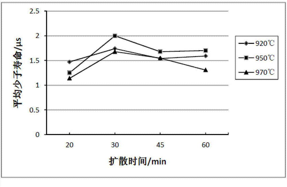
[0052] Table 2 shows the average minority carrier lifetimes of silicon wafers obtained after phosphorus gettering with different diffusion times (20min, 30min, 45min, 60min) at a diffusion temperature of 920°C.

[0053] Table 2

[0054] Diffusion time

[0055] It can be seen from Table 2 that the average minority carrier lifetime can be increased from 0.8 μs to 1.54–1.74 μs after a short time of phosphorus diffusion and gettering for 30–45 min at a diffusion furnace temperature of 920 °C.

Embodiment 3

[0057] Same as Example 1, the difference is that the diffusion temperature in step (3) is 970°C.

[0058] Table 3 shows the average minority carrier lifetimes of silicon wafers obtained after phosphorus gettering with different diffusion times (20min, 30min, 45min, 60min) at a diffusion temperature of 920°C.

[0059] table 3

[0060] Diffusion time

20min

30min

45min

60min

average life expectancy

1.14μs

1.68μs

1.55μs

1.31μs

[0061] It can be seen from Table 3 that the average minority carrier lifetime can be increased from 0.8 μs to 1.55–1.68 μs after short-term phosphorus diffusion and gettering for 30–45 min at a diffusion temperature of 970 °C.

[0062] According to the test result of above-mentioned embodiment 1-3 and with reference to figure 1 It can be seen that, according to the method of the present invention, when the diffusion temperature is 950° C. and the diffusion time is 30 minutes, the average minority car...


PUM

PropertyMeasurementUnit
thicknessaaaaaaaaaa

Abstract

The invention provides a phosphorous gettering method of a metallurgy polycrystalline silicon wafer, a silicon wafer and a solar cell prepared by the silicon wafer The phosphorous gettering method includes: corroding to remove a damaged layer on the surface of the silicon wafer; rinsing the silicon wafer and drying; subjecting the silicon wafer to gettering heat treatment in a diffusion furnace, wherein the diffusion phosphorous source flow volume ranges from 650 to 700ml / min, dry oxygen flow volume ranges from 500 to 700ml / min, diffusing temperature ranges from 920 to 970 DEG C, and the diffusing time ranges from 30-45min; cooling the silicon wafer; corroding to remove a getter layer and PN junctions generated on the surface of the silicon wafer due to phosphorus diffusion; rinsing the silicon wafer and drying to obtain the gettered metallurgy polycrystalline silicon wafer. Service life of the silicon wafer is obviously prolonged, and reverse leakage current and light attenuation of the solar cell prepared by the silicon wafer are obviously reduced. The phosphorous gettering method is short in diffusing time, so that production period is shortened, energy consumption is reduced, and industrial production is suited.

Description

technical field [0001] The invention relates to a gettering method for a polycrystalline silicon wafer, in particular to a method for absorbing phosphorus in a metallurgical polycrystalline silicon wafer, as well as a polycrystalline silicon wafer made by the method and a solar cell made of the polycrystalline silicon wafer. Background technique [0002] With the development of industrialization, non-renewable energy sources such as coal and oil are frequently running out, and energy issues have increasingly become a bottleneck restricting the development of the international society and economy. More and more countries have begun to implement the "Sunshine Plan" to develop solar energy resources and seek new economic development. power. Driven by the huge potential of the international photovoltaic market, the solar cell manufacturing industries of various countries are investing huge sums of money to expand production while continuously researching and developing, explorin...

Claims


Application Information

Patent Timeline
Patent Type & Authority Applications(China)
IPC IPC(8): H01L31/18
CPCY02P70/521Y02P70/50
Inventor 徐志虎谢俊叶倪明镜马承鸿李健和江变蒋西
Owner INNER MONGOLIA RIYUE SOLAR ENERGY TECH
Why Eureka
Try Eureka