Preparation method of high refractive index semiconductor surface anti-reflection passivation composite structure

A high-refractive index, composite structure technology, applied in nanotechnology and other directions, can solve the problems of large reflection loss, low reflectivity, difficult to achieve semiconductor refractive index, etc., to improve efficiency, reduce reflection loss, and improve carrier collection. The effect of efficiency

Active Publication Date: 2013-06-05
SUZHOU INST OF NANO TECH & NANO BIONICS CHINESE ACEDEMY OF SCI
View PDF5 Cites 7 Cited by
  • Summary
  • Abstract
  • Description
  • Claims
  • Application Information

AI Technical Summary

Problems solved by technology

However, for substrate materials with high refractive index (such as Si, GaAs, InP and other semiconductor materials), it is difficult for the commonly used dielectric film materials to match the refractive index of the semiconductor.
Therefore, there is no doubt that there is still a large reflection loss at the interface between the high refractive index material and the dielectric material, which becomes a physical limitation to achieve extremely low reflectivity by this method

Method used


Image

  • Preparation method of high refractive index semiconductor surface anti-reflection passivation composite structure
  • Preparation method of high refractive index semiconductor surface anti-reflection passivation composite structure
  • Preparation method of high refractive index semiconductor surface anti-reflection passivation composite structure

Examples


Embodiment 1

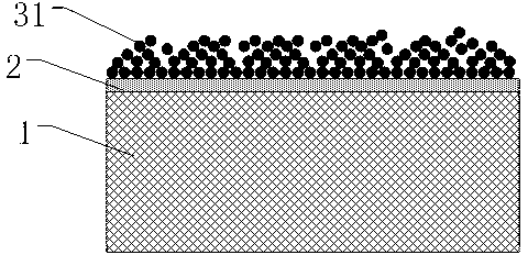
[0027] This embodiment provides a method for preparing a high-refractive index semiconductor surface anti-reflection passivation composite structure. The prepared composite structure is as follows: figure 1 The steps shown are as follows.

[0028]I. Prepare a layer of dense dielectric film 2 for passivating the surface on the surface of the high refractive index semiconductor 1 . Wherein the high refractive index semiconductor includes Si, Ge, III-V group semiconductor, III-N group semiconductor, II-VI group semiconductor and other high refractive index semiconductor materials, and the antireflection passivation composite structure is applied to the solar cell absorption area Surface emission / reception semiconductor optoelectronic devices such as the surface of light-emitting diodes (LEDs), surface-emitting lasers, and detectors. The solar cells include crystalline Si cells, microcrystalline Si cells, amorphous Si and its multi-junction cells, copper indium gallium selenide c...

Embodiment 2

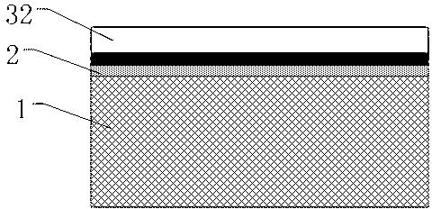
[0035] This embodiment provides a method for preparing a high-refractive index semiconductor surface anti-reflection passivation composite structure. The prepared composite structure is as follows: figure 2 The steps shown are as follows.

[0036] I. Step I is the same as Step I in Example 1.

[0037] II. Deposit metallic titanium on the dielectric film, and form a dielectric titanium oxide nanostructure 32 with a graded refractive index by means of anodic oxidation. It should be noted that: the metal deposited on the dielectric film may be a metal corresponding to a high refractive index dielectric material, at least Ti, Zr, Ta or Y, where titanium and titanium oxide are only provided as examples.

[0038] Among them, the metal titanium film can be prepared by various methods such as thermal evaporation, electron beam evaporation, magnetron sputtering, and atomic layer deposition.

[0039] The properties and functions of the resulting composite structure are as described i...

Embodiment 3

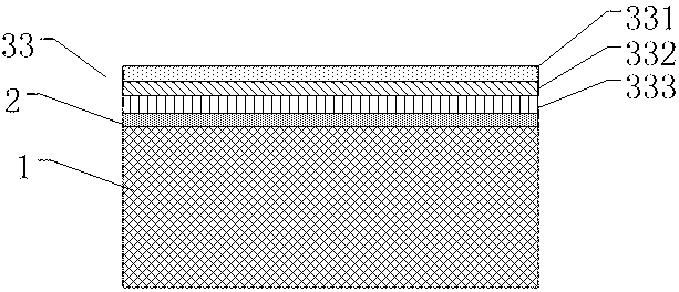
[0041] This embodiment provides a method for preparing a high-refractive index semiconductor surface anti-reflection passivation composite structure. The prepared composite structure is as follows: image 3 The steps shown are as follows.

[0042] I. Step I is the same as Step I in Example 1.

[0043] II. Depositing high-refractive-index dielectric materials with relative refractive index distributions of high, medium and low in sequence on the dielectric film to form a multi-layer composite dielectric layer with a graded refractive index. In this example, the sequentially deposited high-refractive-index dielectric materials are divided into zirconia, silicon nitride and silicon oxide thin films according to the high, medium and low relative refractive indices, forming a multi-layer composite dielectric layer 33 with a graded refractive index.

[0044] Deposit dielectric films 333, 332 and 331 in sequence on the dense dielectric film prepared in step 1, wherein 333 refers to ...


PUM

PropertyMeasurementUnit
refractive indexaaaaaaaaaa

Abstract

The invention discloses a preparation method of a high refractive index semiconductor surface anti-reflection passivation composite structure. The method comprises: I, a layer of dielectric film used for a passivated surface is prepared on the surface of a semiconductor; and II, a dielectric layer with gradual refractive index based on dielectric materials with a high refractive index is prepared on the dielectric film, dielectric materials materials with high refractive index select one type or several types from SiN, HfO2, TiO2, ZrO2, Ta2O5 and Y203according to semiconductor materials which need to be matched and the wavelength range of needed anti-reflection, and an anti-reflection passivation composite structure is combined by the dielectric film and the dielectric layer with the gradual refractive index. According to the preparation method, non-radiative recombination on the surface of the semiconductor is reduced, reflection loss is reduced, charge collection efficiency is effectively improved, and the function of wide spectrum wide angle anti-reflection is achieved.

Description

technical field [0001] The invention relates to a method for preparing a dielectric film on a semiconductor surface with a graded refractive index, and more specifically, to a method for preparing a composite structure for antireflection and passivation on a semiconductor surface with a high refractive index suitable for solar cells, which belongs to micro-nano photon technology field. Background technique [0002] The interface reflectivity between substances with different refractive index is an important parameter that affects the performance of receiving light, emitting light, and transmitting optical devices and equipment. Extremely low interface reflectivity is the pursuit of light display, broadband light source, solar cells, lenses and other fields. Important indicators. Usually, the method of evaporating an optical anti-reflection film is used to reduce the reflection of the optical interface. In order to reduce the interface reflectance as far as possible in a wi...

Claims


Application Information

Patent Timeline
Patent Type & Authority Applications(China)
IPC IPC(8): C23F17/00B82Y40/00
Inventor 张瑞英
Owner SUZHOU INST OF NANO TECH & NANO BIONICS CHINESE ACEDEMY OF SCI
Why Eureka
Try Eureka