Polishing solution for TSV barrier layer

A technology of polishing liquid and barrier layer, applied in the field of polishing liquid, to achieve the effect of clear and sharp thin line area, good planarization efficiency and good corrosion resistance

Active Publication Date: 2013-06-12
ANJI MICROELECTRONICS TECH (SHANGHAI) CO LTD
View PDF15 Cites 6 Cited by
  • Summary
  • Abstract
  • Description
  • Claims
  • Application Information

AI Technical Summary

Problems solved by technology

[0003] There are many ways to integrate the TSV process, but they all face a common problem, that is, TSV production needs to break through different material layers, including silicon materials, various insulating or conductive film layers in ICs
No commercial TSV barrier polishing fluids have been reported so far

Method used


Image

  • Polishing solution for TSV barrier layer
  • Polishing solution for TSV barrier layer
  • Polishing solution for TSV barrier layer

Examples


Embodiment Construction

[0029] The advantages of the present invention will be further elaborated below through specific embodiments.

[0030] Polishing conditions:

[0031] Polishing pad: IC pad

[0032] Polishing conditions: 70 / 90rpm

[0033] Polishing fluid flow: 100ml / min

[0034] Static corrosion rate: Put the freshly polished copper sheet into the slurry and immerse it for 15 minutes, and measure the film thickness before and after.

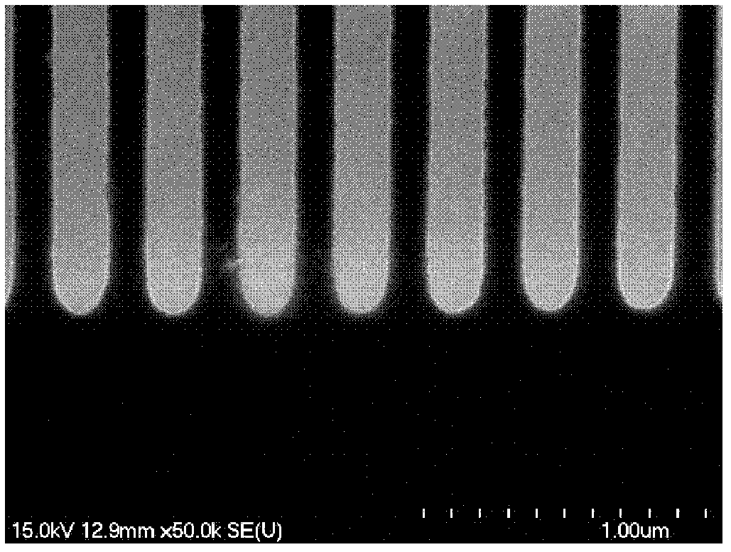
[0035] Butterfly Depression: A Semitech 854 patterned wafer was used to measure the butterfly depression of an 80um metal block.

[0036] Polishing Uniformity Within Slice: Butterfly dips for different line widths within a die.

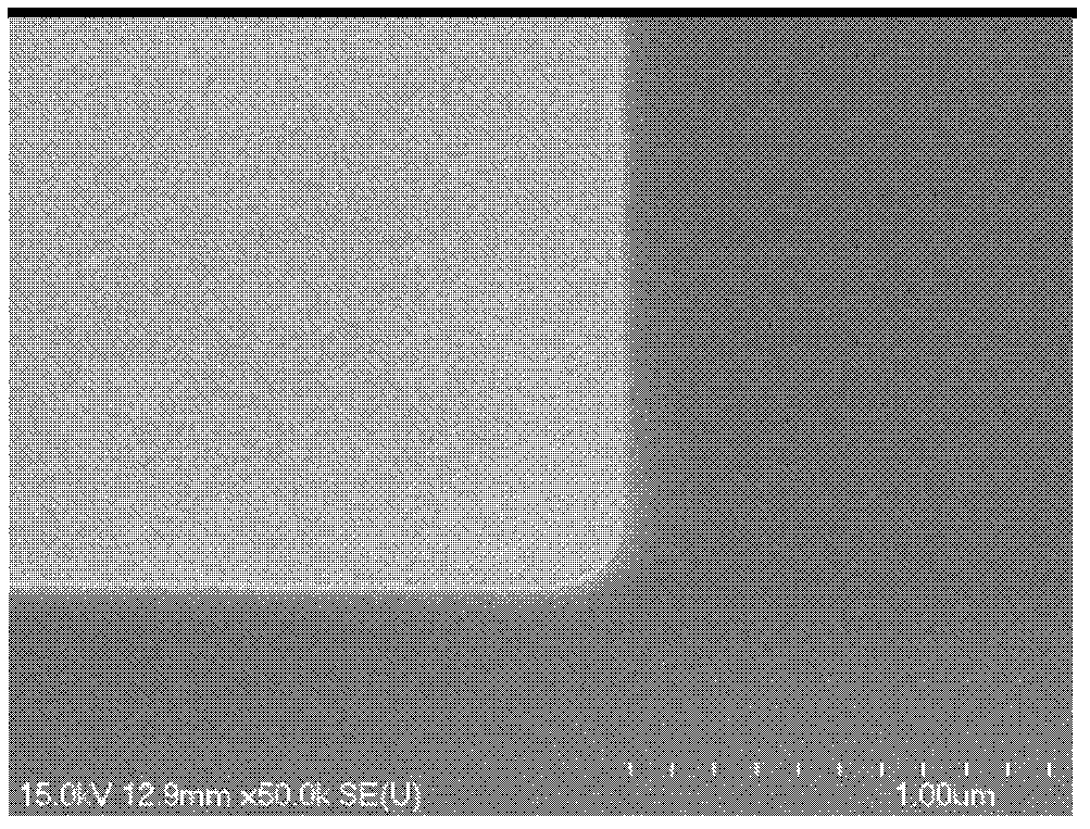
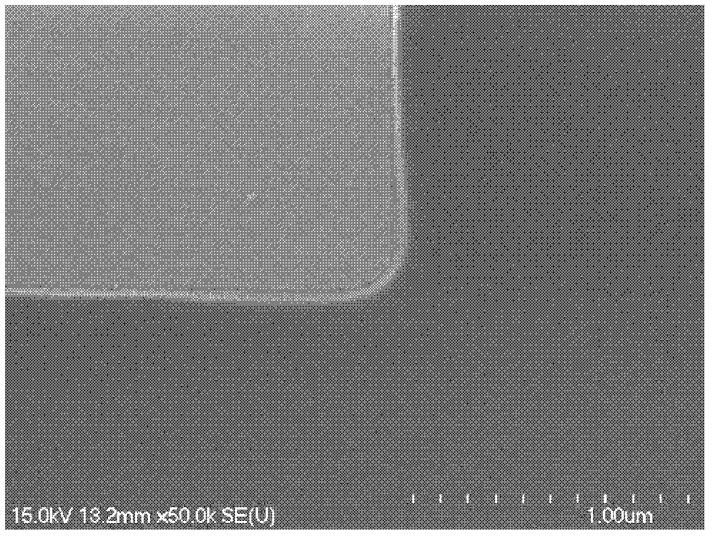
[0037] Blank Wafer: PETEOS, Ta, Cu, Si3N4

[0038] Table 1, the formula of embodiment 1-7 and contrast polishing liquid

[0039]

[0040]

[0041] BTA: benzotriazole, PAA: polyacrylic acid, PBTCA: 2-phosphonic acid-1,2,4-tricarboxylic butane. DISN1, disodium methylene bis-naphthalenesulfonate, DISN2: methylnaphthalenesulfonat...


PUM

PropertyMeasurementUnit
particle diameteraaaaaaaaaa

Abstract

The invention discloses a chemical-mechanical polishing solution for a through silicon via (TSV) barrier layer. The polishing solution comprises at least one grinding material, a compound metal copper corrosion inhibitor, a complexing agent and a silicon nitride regulator. The polishing solution has relatively high silica removal rate and relatively low silicon nitride removal rate, can planarize the barrier layer efficiently and stop the silicon nitride layer to form the through silicon via (TSV), does not produce metal corrosion, and has relatively high defect correction capability and relatively low surface contamination index.

Description

technical field [0001] The invention relates to a polishing liquid, in particular to a chemical mechanical polishing liquid for polishing a TSV barrier layer. Background technique [0002] see Figure 5-7 , in order to improve the performance of IC, further reduce the size, reduce power consumption and cost, small size 3D TSV (TSV, Through-Silicon-Via) packaging technology has emerged as the times require. 3D TSV is the latest technology to realize the interconnection between chips by making vertical conduction between chips and between wafers. Unlike previous IC package bonding and overlay technologies using bumps, TSV can maximize the density of chips stacked in three dimensions and minimize the overall size, greatly improving the performance of chip speed and low power consumption. Its main advantages are: having the smallest size and weight, integrating different kinds of technologies into a single package, replacing long 2D interconnects with short vertical interconnec...

Claims


Application Information

Patent Timeline
Patent Type & Authority Applications(China)
IPC IPC(8): C09G1/02
CPCC09G1/02C09K3/1454H01L21/3212H01L21/30625C09K3/1463H01L21/76898
Inventor 宋伟红姚颖孙展龙
Owner ANJI MICROELECTRONICS TECH (SHANGHAI) CO LTD
Why Eureka
Try Eureka