Thick-film anti-vulcanization paster resistor and manufacturing method thereof

A technology for chip resistors and manufacturing methods, applied in resistor manufacturing, resistors, resistor components and other directions, can solve the problems of excessive cost, high cost, different expansion coefficients, etc., to improve anti-sulfurization performance and reduce production costs , the effect of prolonging the vulcanization path

Active Publication Date: 2013-06-19
UNIROYAL ELECTRONICS IND
View PDF2 Cites 19 Cited by
  • Summary
  • Abstract
  • Description
  • Claims
  • Application Information

AI Technical Summary

Problems solved by technology

The reason why the anti-sulfurization ability of the chip resistor is not strong is mainly due to the following disadvantages in the material and product structure: the nickel-plated layer 40 and the tin-plated layer 50 are directly overlapped on the edge of the second protective layer 28, while the second protective layer 28 The material of the second protective layer is usually a resin material. When the customer performs wave soldering or reflow soldering on the chip resistor on the PCB, the expansion coefficient of the nickel plating laye...

Method used


Image

  • Thick-film anti-vulcanization paster resistor and manufacturing method thereof
  • Thick-film anti-vulcanization paster resistor and manufacturing method thereof
  • Thick-film anti-vulcanization paster resistor and manufacturing method thereof

Examples


Embodiment 1

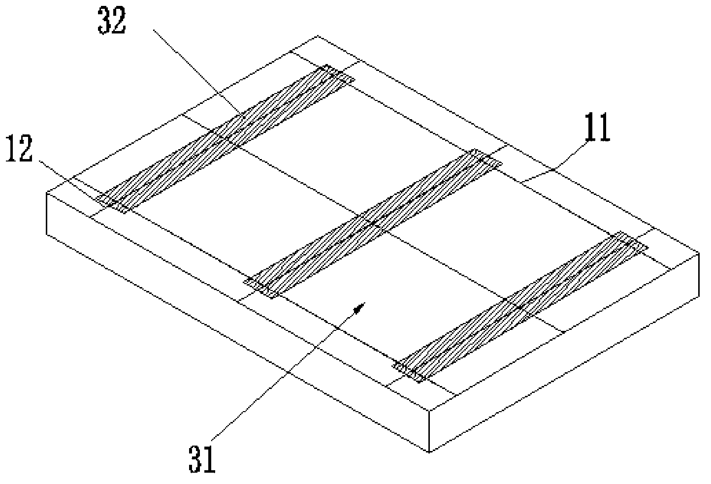
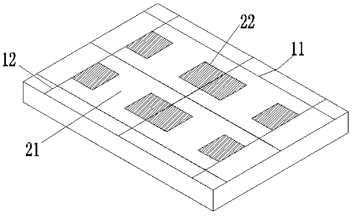
[0066] Such as Figure 15 and 16 As shown, a thick-film anti-sulfurization chip resistor includes a square insulating substrate. Based on the direction of use, the lower surfaces of both ends of the insulating substrate are respectively covered with a layer of back electrodes 32; the upper surfaces of both ends of the insulating substrate are respectively covered with a layer of The first front electrode 22, the upper surface of the insulating substrate between the two first front electrodes is covered with a layer of resistance layer 23, the two first front electrodes are covered with a layer of second front electrode 24, and then covered on the resistance layer in turn The first protective layer 25 and the second protective layer 28; both ends of the resistance layer respectively extend to cover a part of the first front electrode; the second front electrode extends to cover a part of the resistance layer and a part of the first protective layer; the second The protective l...

Embodiment 2

[0073] Such as Figure 17 As shown, this embodiment includes all the technical features in Embodiment 1, the difference is that a third front electrode 27 is additionally provided, the third front electrode is located between the second front electrode and the nickel plating, and the third front electrode extends Select one to cover a part of the resistive layer and a part of the first protection layer.

[0074] By adding the third front electrode on the second front electrode, an overlapping and staggered structure of the first front electrode and the resistance layer, the second front electrode, the third front electrode and the first protection layer is formed. The specific overlapping and staggered structure can be as follows: the resistance layer extends and extends to cover a part of the first front electrode, then the second front electrode extends to cover a part of the resistance layer, the first protective layer extends to cover a part of the second front electrode, ...


PUM


Abstract

The invention discloses a thick-film anti-vulcanization paster resistor and a manufacturing method thereof. A second front side electrode is added to a first front side electrode so as to form an overlapped and intersected structure of the second front side electrode and a resistor layer as well as the second front side electrode and a first protecting layer; and the expansion coefficient of a second protecting layer is matched with that of the second front side electrode. Due to the structural method design, a vulcanization route is greatly prolonged, so that the anti-vulcanization property of the paster resistor is improved, and moreover, the phenomenon that the electrode is corroded by vulcanization gas from cracks caused in wave peak soldering or reflow soldering of a PCB (Printed Circuit Board) of the resistor because of the difference of expansion coefficients of an electro-nickelling layer, an electro-tinning layer and the second protecting layer. Therefore, the production cost of the thick-film anti-vulcanization paster resistor is greatly lowered, and the thick-film anti-vulcanization paster resistor can be widely applied to ordinary electronic products.

Description

technical field [0001] The invention relates to a resistor and a manufacturing method thereof, in particular to a thick-film anti-sulfurization chip resistor and a manufacturing method thereof. Background technique [0002] Chip resistors, also known as chip resistors, are small in size, light in weight, suitable for reflow soldering and wave soldering, stable in electrical performance, high in reliability, low in assembly cost, and match with automatic mounting equipment, high in mechanical strength and It is widely used in computers, mobile phones, electronic dictionaries, medical electronic products, camcorders, electronic watt-hour meters and VCD players due to its superior high-frequency characteristics. However, in some occasions where the concentration of sulfide gas is high, such as places where volcanic gas is emitted, farms, wine brewing, parking lots, chemical plants, mining and thermal power plants, etc., electronic equipment using chip resistors often produce su...

Claims


Application Information

Patent Timeline
IPC IPC(8): H01C7/00H01C1/148H01C1/02H01C17/00H01C17/02H01C17/28
Inventor 彭荣根徐玉花杜杰霞王晨
Owner UNIROYAL ELECTRONICS IND
Why Eureka
Try Eureka