Vertical parasitic type plug-and-play (PNP) audion in germanium silicon heterojunction bipolar transistor (HBT) technology and manufacture method

A PNP triode and vertical parasitic technology, which is applied in semiconductor/solid-state device manufacturing, electrical components, circuits, etc., can solve the problems of low emission coefficient of PNP triode, inability to penetrate the germanium-silicon alloy carbon layer, and insufficient cut-off frequency to achieve improvement Effects of parasitic effects, area saving, improvement of current gain coefficient and frequency characteristics

Active Publication Date: 2013-06-19
SHANGHAI HUAHONG GRACE SEMICON MFG CORP
View PDF5 Cites 2 Cited by
  • Summary
  • Abstract
  • Description
  • Claims
  • Application Information

AI Technical Summary

Problems solved by technology

Therefore, although the doping dose of the emitter region of the existing PNP triode is very large, because the energy is very small, it is impossible to break through the carbon layer in this layer of germanium-silicon alloy, causing most of the boron to be suppressed in the emitter region The region of a SiGe single crystal very close to the surface
And because the emitter region of the existing PNP transistor needs to grow a layer of metal silicide in the subsequent process, the heavily doped region of the surface of the germanium-silicon single crystal in the emitter region is mostly consumed, so that the existing The emission coefficient of the PNP transistor is very low, resulting in a low device amplification factor, and the cut-off frequency is not high enough

Method used


Image

  • Vertical parasitic type plug-and-play (PNP) audion in germanium silicon heterojunction bipolar transistor (HBT) technology and manufacture method
  • Vertical parasitic type plug-and-play (PNP) audion in germanium silicon heterojunction bipolar transistor (HBT) technology and manufacture method
  • Vertical parasitic type plug-and-play (PNP) audion in germanium silicon heterojunction bipolar transistor (HBT) technology and manufacture method

Examples


Embodiment Construction

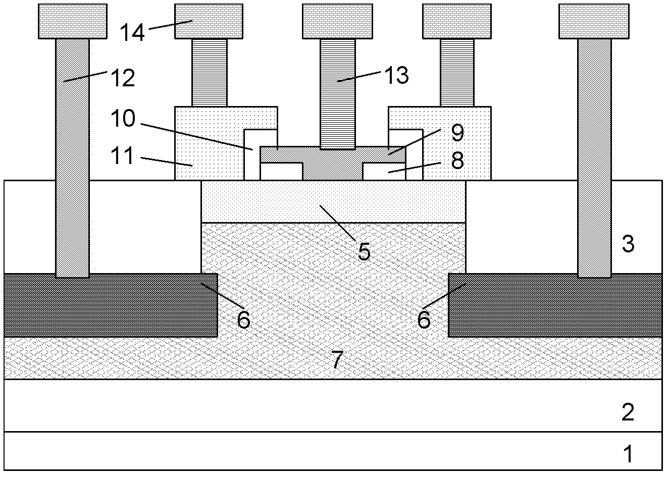
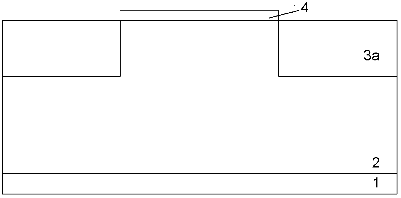
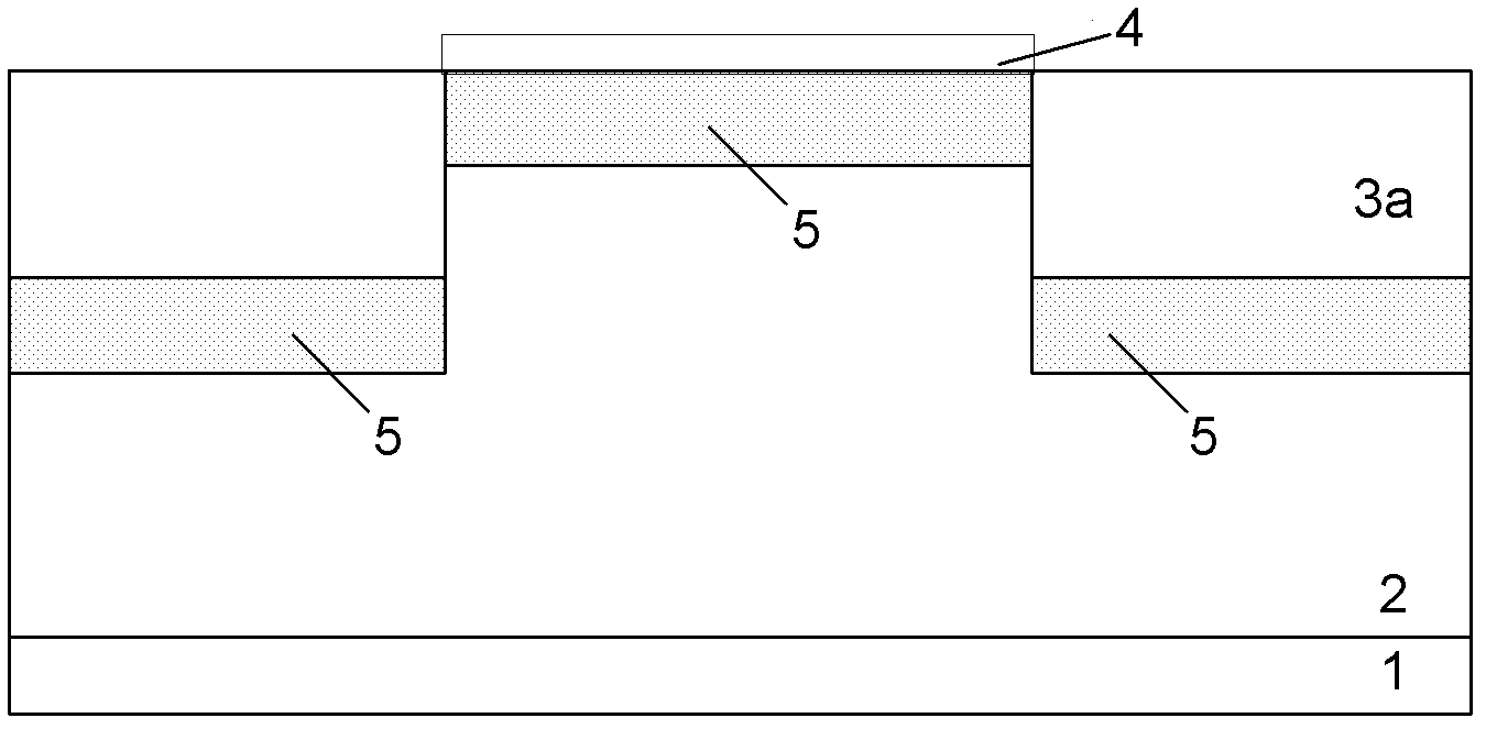
[0043] Such as figure 1 Shown is a schematic structural diagram of a vertical parasitic PNP transistor in the silicon germanium HBT process of the embodiment of the present invention. In the silicon germanium HBT process of the embodiment of the present invention, the vertical parasitic PNP transistor is formed on the P-type silicon substrate 1, and an N-type deep well 2 is formed on the P-type silicon substrate 1, and the active region is composed of a shallow groove field oxygen 3 isolation is shallow trench isolation (STI), including:

[0044] A collector region 7 is composed of a P-type ion implantation region formed in the active region, and the depth of the collector region 7 is greater than or equal to the depth of the bottom of the shallow trench field oxygen 3 . The P-type ion implantation in the collector region adopts the CMOS P-well implantation process in the SiGe HBT process.

[0045] A pseudo-buried layer 6, composed of P-type ion implantation regions formed a...


PUM


Abstract

The invention discloses a vertical parasitic type plug-and-play (PNP) audion in a germanium silicon heterojunction bipolar transistor (HBT) technology. A window defining germanium before growth in a trapezoid shape is adopted and germanium silicon layers in an emitter region can be in a polycrystalline structure, and therefore dosage concentration in the emitter region can be improved, emitting efficiency and amplification coefficient of a device is improved, and cut-off frequency of the device is increased. Due to the fact that the advanced deep hole contact technology and the P-type buried layer technology are adopted, area of an active region can be greatly saved, parasitic effect of the device is improved, collector resistance of the device is reduced, and performance of the device is improved. The invention further discloses a manufacture method of the vertical parasitic type PNP audion in the germanium silicon HBT technology. The manufacture method can be integrated with the technology of the PNP audion in the germanium silicon HBT technology and reduce production cost.

Description

technical field [0001] The invention relates to the field of semiconductor integrated circuit manufacturing, in particular to a vertical parasitic PNP transistor in a silicon-germanium HBT process, and also relates to a method for manufacturing a vertical parasitic PNP transistor in a silicon-germanium HBT process. Background technique [0002] In the practical application of radio frequency products, higher and higher device characteristic frequencies are required. In the BiCMOS process, NPN transistors, especially silicon germanium (SiGe) heterojunction transistors (HBT) or germanium silicon carbon (SiGeC) heterojunction transistors are good choices for UHF devices. And the SiGe process is basically compatible with the silicon process, so SiGe HBT has become one of the mainstreams of UHF devices. In this context, the requirements for the output device are correspondingly increased, such as having a certain current gain coefficient (not less than 15) and cut-off frequency....

Claims


Application Information

Patent Timeline
Patent Type & Authority Applications(China)
IPC IPC(8): H01L29/737H01L29/06H01L29/08H01L21/331
Inventor 陈帆陈雄斌刘冬华薛恺周克然潘嘉李昊蔡莹陈曦
Owner SHANGHAI HUAHONG GRACE SEMICON MFG CORP
Why Eureka
Try Eureka