Band-gap adjustable micro-strip ultra-wide band filter

An ultra-wideband filter and microstrip technology, which is applied in waveguide devices, electrical components, circuits, etc., can solve the problems of non-adjustable, wide bandwidth, and occupied communication frequency bands, so as to reduce the size, increase the degree of freedom, and improve the utilization of frequency bands. rate effect

Inactive Publication Date: 2013-07-03
西安伊艾姆科技有限公司
View PDF1 Cites 26 Cited by
  • Summary
  • Abstract
  • Description
  • Claims
  • Application Information

AI Technical Summary

Problems solved by technology

In March 2008, H.R.Arachchige and others published "UWB Bandpass Filter with Tunable Notch on Liquid Crystal Polymer Substrate" on Microwave Conference.2008 (APMC2008).Asia-Pacific (Dec.16-20,pp.1-4,2008). ", proposed a bandgap tunable ultra-wideband filter, which can realize a continuously adjustable bandgap, but the bandgap width increases with the increase of frequency, which will occupy the effective communication frequency band; 2011 In January 2011, Feng Wei et al published "Compact UWB Bandpass Filter With Dual Notched Bands Based on SCRLH Resonator" in IEEE Transactions on Microwave Theory and Techniques journal (vol.21, no.1, pp.28-30, 2011) , a novel dual-bandgap ultra-wideband filter is proposed, which has two fixed-frequency bandgaps, but both bandgaps are not adjustable, and the bandwidth is wider

Method used


Image

  • Band-gap adjustable micro-strip ultra-wide band filter
  • Band-gap adjustable micro-strip ultra-wide band filter
  • Band-gap adjustable micro-strip ultra-wide band filter

Examples


Embodiment 1

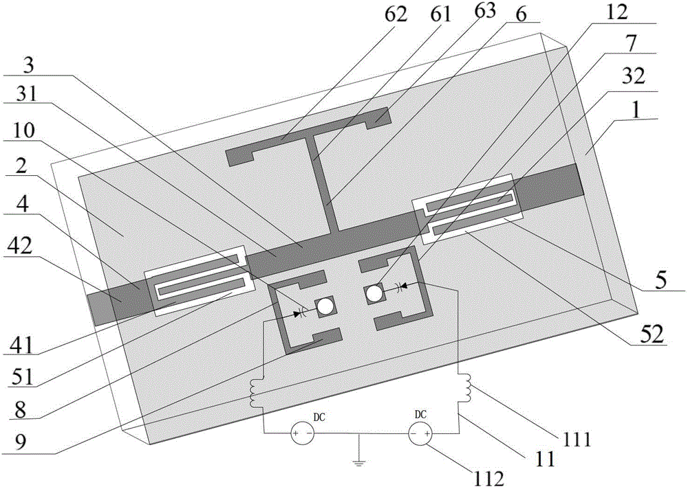
[0034] The present invention mainly consists of a microstrip dielectric substrate 1, a metal ground plate 2, a multimode resonator 3, a pair of input and output interdigitated microstrip feeders 4, a defective ground structure 5, a "T"-shaped branch 6, and a bandgap resonator 7. Varactor diode 10, DC bias circuit 11 and grounding hole 12, wherein:

[0035] The microstrip dielectric substrate 1 adopts a single-sided copper-clad dielectric substrate with a dielectric constant of 2.65 and a thickness of 1 mm;

[0036] The metal ground plate 2 is arranged on the lower surface of the microstrip dielectric substrate 1;

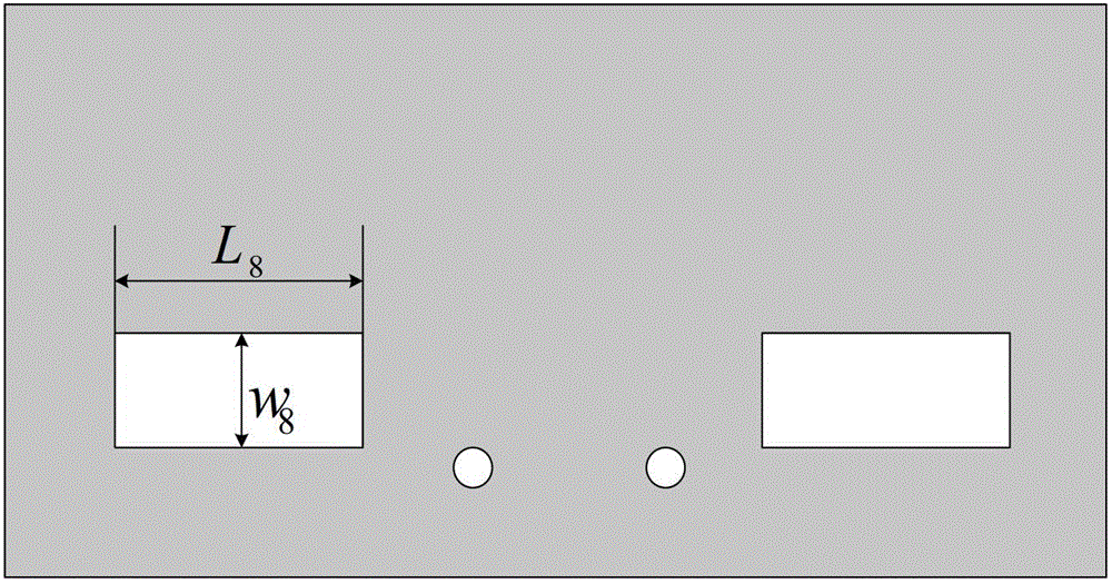
[0037] The defective ground structure 5 and the ground hole 12 are arranged on the lower surface of the metal ground plate 2, and the ground hole 12 is located at the lower middle position of the defective ground structure 5;

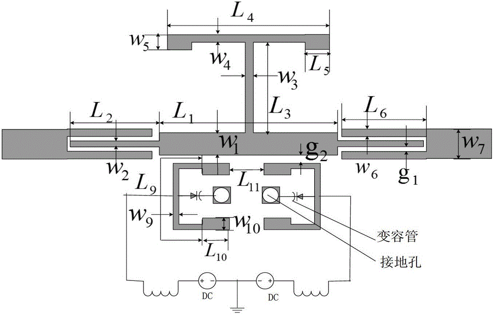
[0038] The multimode resonator 3 is arranged on the upper surface of the microstrip dielectric substrate 1, and has a length L 1 , with a ...

Embodiment 2

[0056] The structure of this example is identical with embodiment 1, and the parameter value design different from embodiment 1 is as follows:

[0057] The bandgap resonator 7 is located below the multimode resonator 3, and the gap width g between the bandgap resonator 7 and the multimode resonator 3 211 Satisfied: 011 1 -2L 10 ), each ladder impedance resonator is composed of high impedance line 8 and low impedance line 9, and w 9 9 5,w 10 9 5,w 9 10 ,

[0058] in, is the operating wavelength when the bandgap resonator operates at the fundamental frequency, c is the speed of light in vacuum, is the effective permittivity of the bandgap resonator, is the fundamental frequency of the bandgap resonator.

[0059] In this example, the length L of the high-impedance line 8 is taken 9 =6.5mm, width w 9 =0.3mm, the length L of the low impedance line 9 10 =2.7mm, width w 10 =1.0mm, the corresponding resonant frequency The distance L between the two stepped impeda...

Embodiment 3

[0062] The structure of this example is identical with embodiment 1, and the parameter value design different from embodiment 1 is as follows:

[0063] The bandgap resonator 7 is located below the multimode resonator 3, and the gap width g between the bandgap resonator 7 and the multimode resonator 3 2 11 Satisfied: 011 1 -2L 10 ), each ladder impedance resonator is composed of high impedance line 8 and low impedance line 9, and w 9 9 / 5,w 10 9 / 5,w 9 10 ,

[0064] in, is the operating wavelength when the bandgap resonator operates at the fundamental frequency, c is the speed of light in vacuum, is the effective permittivity of the bandgap resonator, is the fundamental frequency of the bandgap resonator.

[0065] In this example, the length L of the high-impedance line 8 is taken 9 =6.5mm, width w 9 =0.4mm, the length L of the low impedance line 9 10 =2.9mm, width w 10 =1.1mm, the corresponding resonant frequency The distance L between the two stepped imp...


PUM


Abstract

The invention discloses a band-gap adjustable micro-strip ultra-wide filter, which is mainly used for solving the problems that the band-gap loading ultra-wide filter has out-of-band suppression difference, bigger band gap width and independent turning of double band gaps. The filter comprises a micro-strip medium substrate (1), a metal grounding plate (2), a multi-mode resonator (3), a pair of input-output interdigital micro-strip feeder lines (4), a defected ground structure (5) and a direct-current biasing circuit (11), wherein a T-shaped branch (6) is loaded in the center of the multi-mode resonator (3); a band gap resonator (7) is loaded on the lower surface of the multi-mode resonator (3); the band gap resonator consists of two symmetrical stepped-impedance resonators (71, 72) and a variode (10); and capacitance value of the variode (10) is controlled by adjusting the biasing voltage of the direct-current biasing circuit (11). The band-gap adjustable micro-strip ultra-wide band filter is small in dimension, narrow in band gap width, good in out-of-band suppression difference, is capable of realizing continuous adjustment of the first band gap, is capable of keeping the second band gap constant and can be used for a wireless communication system.

Description

technical field [0001] The invention belongs to the technical field of electronic devices, and in particular relates to an adjustable microstrip ultra-wideband filter, which can be used for a radio frequency front end of a wireless communication system. Background technique [0002] With the rapid development of wireless communication technology, people's requirements for information technology are getting higher and higher. Ultra-wideband UWB technology has the advantages of simple system, low power consumption, good concealment, strong multipath resolution ability, fast data transmission rate and low cost. , high security and other advantages, making it a research hotspot in the field of wireless communication. The communication frequency range of the UWB system is 3.1GHz to 10.6GHz. Due to its wide frequency band, the frequency band overlaps with some narrowband systems, such as the WiMAX system with a frequency of 3.5GHz and the WLAN system with a frequency range of 5.2G...

Claims


Application Information

Patent Timeline
Patent Type & Authority Applications(China)
IPC IPC(8): H01P1/203
Inventor 吴边张小艳邱枫孙守家张灵芝
Owner 西安伊艾姆科技有限公司
Why Eureka
Try Eureka