Vapor plating method for organic light-emitting diode

A luminescence and diode technology, which is applied in the evaporation field of organic electroluminescent diodes, can solve the problems of inaccessible substrates, etc., and achieve the effects of improving service life, increasing utilization rate, and avoiding deformation of the board surface

Inactive Publication Date: 2013-07-17
KUN SHAN POWER STENCIL
View PDF5 Cites 0 Cited by
  • Summary
  • Abstract
  • Description
  • Claims
  • Application Information

AI Technical Summary

Problems solved by technology

[0014] The technical problem to be solved by the present invention is that in the existing OLED manufacturing technology, the organic particles cannot reach the substrate due to the shielding of the opening wall during evaporation, and a new evaporation method is provided, which has the utilization rate of organic materials. High, high film formation rate, long service life of mask plate, cost saving advantages

Method used


Image

  • Vapor plating method for organic light-emitting diode
  • Vapor plating method for organic light-emitting diode
  • Vapor plating method for organic light-emitting diode

Examples


Embodiment 1

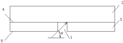
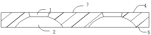
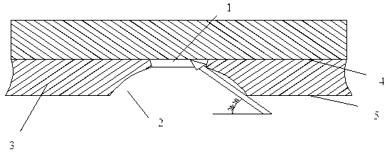
[0035] A mask for evaporation, such as figure 2 As shown, the thickness is 50 μm and the shape is a quadrilateral metal plate, which includes an ITO surface 4 and an evaporation surface 5 in contact with indium tin oxide (ITO). The mask plate has through holes that penetrate the ITO surface and the evaporation surface. The size of the opening 1 of the through hole on the ITO surface is smaller than the size of the opening 2 on the vapor deposition surface. Invar alloy is selected as the mask material, and the double-sided etching process is adopted. image 3 It is a schematic diagram of mask and ITO surface matching.

[0036] Etch from the ITO surface 4 of the mask to form as figure 2 The opening 1 on the ITO surface of the middle mask has a depth of 15μm and a lateral dimension of 70μm. It is etched from the vapor deposition surface 5 of the mask to form as figure 2 The opening 2 on the middle vapor deposition surface, and ensure that the opening 2 on the vapor deposition surf...

Embodiment 2

[0040] A mask for vapor deposition, with a thickness of 100 μm and a quadrilateral metal plate, including two surfaces, an ITO surface in contact with indium tin oxide (ITO) and a vapor deposition surface. The mask has a through ITO surface and a vapor deposition surface. The size of the opening on the ITO surface of the through hole of the plating surface is smaller than the size of the opening on the vapor deposition surface.

[0041] The vapor deposition mask is a quadrilateral nickel-cobalt alloy metal plate. The ITO surface of the mask has an opening depth of 35 μm and a lateral dimension of 70 μm. The opening on the vapor deposition surface coincides with the center of the ITO surface opening of the template, and the vapor deposition surface The center of the opening is symmetrical, the depth is 65 μm, the lateral dimension is 140 μm, and the wall of the opening on the evaporation surface has a certain concave arc, forming an evaporation angle of 30°. By separately controll...


PUM

PropertyMeasurementUnit
thicknessaaaaaaaaaa
thicknessaaaaaaaaaa

Abstract

The invention relates to a vapor plating method for an organic light-emitting diode (OLED), and aims to mainly solve the technical problem that organic particles cannot reach a substrate due to shadowing of a mask plate aperture wall during vapor plating in the existing OLED manufacturing technologies. The invention employs a diode vapor plating method, which includes the steps of: combining the ITO (indium tin oxide) surface of a mask plate with an ITO semiconductor glass surface, making the vapor plating surface of the mask plate correspond to an organic vapor plating source; vaporizing an?organic material, and making the organic material attached to the ITO semiconductor glass surface through through-holes on the mask plate; and separating the mask plate and the ITO semiconductor glass, thus completing vapor plating. Specifically, by adopting the technical scheme that the aperture size of the through-holes on the ITO surface is smaller than that on the vapor plating surface, the problem is well solved. Thus, the method provided in the invention can be used in the industrial production of organic light-emitting diodes.

Description

[0001] technical field [0002] The invention relates to an evaporation method for an organic electroluminescent diode. [0003] Background technique [0004] Generally, an OLED device is an emissive display device that emits light by electrically exciting a fluorescent organic compound. The OLED device can be regarded as a passive matrix OLED (PMOLED) device or an active matrix OLED (AMOLED) device according to a driving manner of N×M pixels that can be arranged in a matrix. Compared with PMOLED devices, AMOLED devices are suitable for large-sized displays due to their low power consumption and high resolution. [0005] Depending on the direction in which light is emitted from the organic compound, the OLED device can be a top-emitting OLED device, a bottom-emitting OLED device, or a top and bottom-emitting OLED device. Top-emitting OLED devices emit light in the opposite direction to the substrate on which the pixels are disposed and, unlike bottom-emitting OLEDs, have ...

Claims


Application Information

Patent Timeline
Patent Type & Authority Applications(China)
IPC IPC(8): C23C14/04H01L51/56
Inventor 魏志凌高小平郑庆靓
Owner KUN SHAN POWER STENCIL
Why Eureka
Try Eureka