

Composite semi-conductor integrated circuit with three-dimensional element
A technology of three-dimensional components and integrated circuits, which is applied to semiconductor devices, semiconductor/solid-state device components, circuits, etc., and can solve problems such as component damage and component performance reduction.
- Summary
- Abstract
- Description
- Claims
- Application Information
AI Technical Summary
Problems solved by technology
Method used
Image

Examples
Embodiment Construction
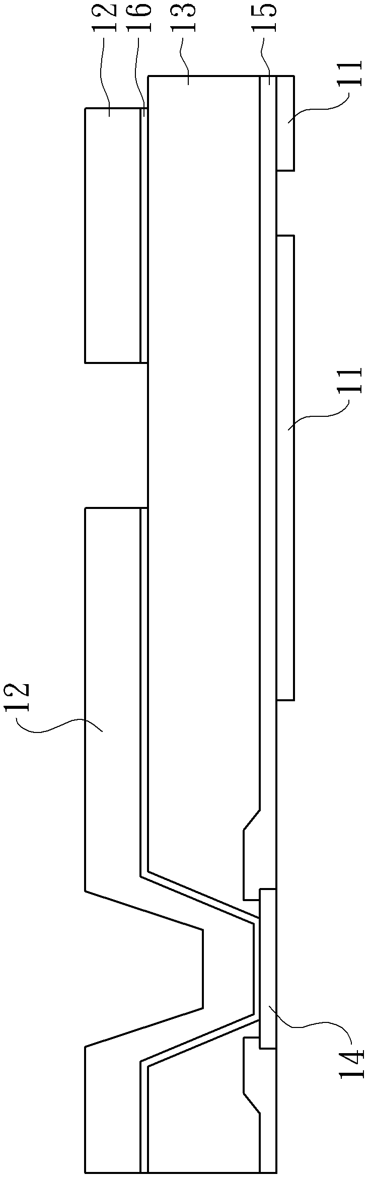
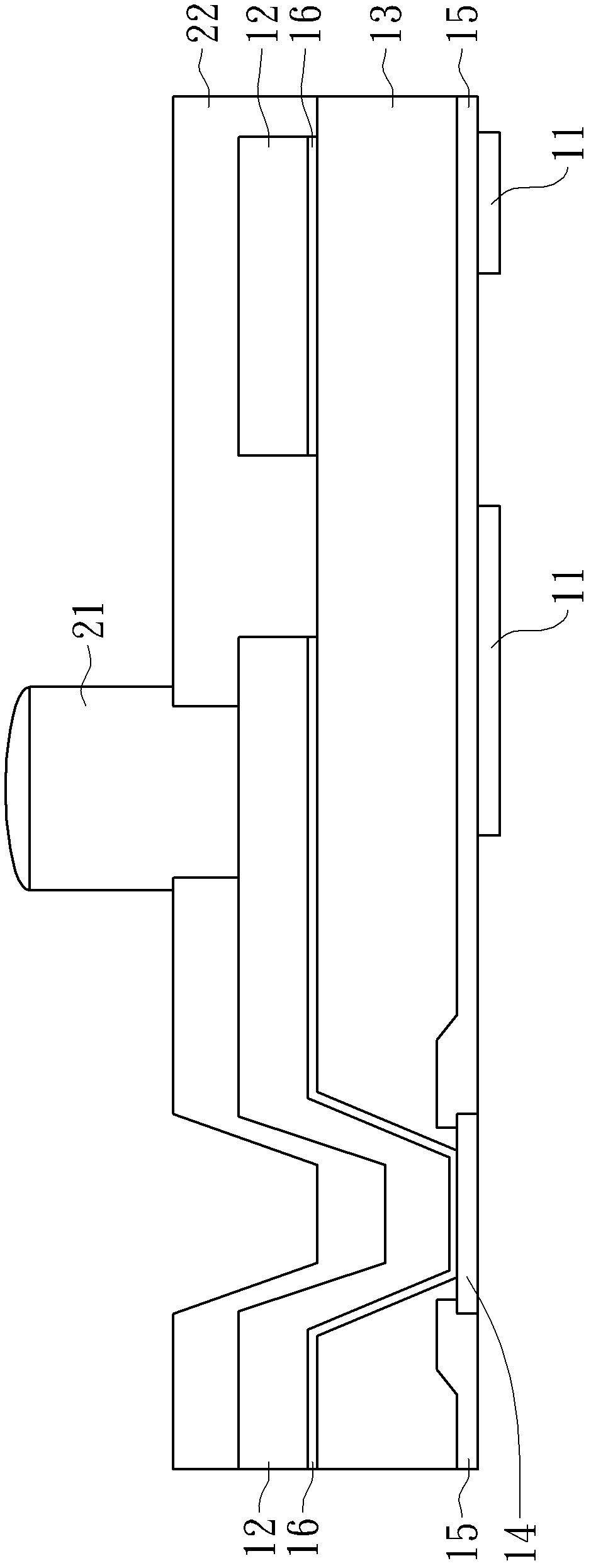
[0026] figure 1 It is a cross-sectional schematic view of the composite semiconductor integrated circuit of the present invention, which includes at least one electronic component 11, a pad 12 located above the electronic component 11, and a first dielectric layer 13 inserted between the two as an electrical component. isolation. The electronic element 11 is formed on a composite semiconductor substrate, among which a semi-insulating gallium arsenide substrate is preferred. The electronic component 11 can be a high electron mobility transistor (HEMT), a heterojunction bipolar transistor (HBT), a thin film resistor (TFR), a diode, a metal-insulator-metal capacitor (MIM) Or a metal-insulator-metal capacitor stack.
[0027] The thickness of the first dielectric layer 13 between the electronic component 11 and the pad 12 is between 10 and 30 microns. The thickness within this range is enough to effectively reduce the coupling capacitance between the electronic component 11 and ...
PUM
| Property | Measurement | Unit |
|---|---|---|
| Thickness | aaaaa | aaaaa |
Abstract
Description
Claims
Application Information