


Quick Research
Generate reliable direction feasibility study reports for your R&D in just a few steps.

Technical Q&A
Discover and master advanced knowledge NOW. Basics, ideas, possibilities, all at once.

Find Solutions
As an expert in R&D theories, this can generate solutions to your technical problems instantly.

Evaluate Feasibility
Analyze your overall solution with one click, know your potential R&D risks in advance.

Monitor Landscape
Get weekly tech updates, stay abreast of the latest tech innovations and key insights.
Preparation method of graphene radiating fins
A technology of graphene and heat sink, which is applied in the field of microelectronic packaging, can solve problems that affect the electrical performance, mechanical strength and reliability of the chip, reduce the stability of the chip, and increase the error rate.
- Summary
- Abstract
- Description
- Claims
- Application Information
AI Technical Summary
Problems solved by technology
Method used
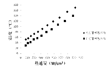
Image


Examples
Embodiment 1
[0011] (1) Deposit a layer of copper with a thickness of 1 micron on the surface of silicon dioxide by conventional electron beam evaporation method, and the purity of copper is 99.9%.
[0012] (2) Pass acetylene, hydrogen and argon into the reaction chamber of the Aixtron Black Magic deposition system, react at 900 degrees Celsius for 5-10 minutes, and grow graphene on the surface of silicon dioxide deposited with copper by chemical vapor deposition , The flow ratio of acetylene and hydrogen is 1:2 to 1:4, and the flow rate of acetylene is 5~10 standard cubic centimeters per minute (sccm).
[0013] (3) After cooling, spin-coat a layer of 300nm polymethyl methacrylate on the copper surface.
[0014] (4) Use 30% ferric chloride to etch copper for 20 minutes.
[0015] (5) Transfer the graphene spin-coated with polymethyl methacrylate to the target chip.
[0016] (6) The polymethyl methacrylate was removed with acetone, and finally the graphene heat sink was obtained.
PUM
 Abstract
Description
Claims
Application Information
 - R&D Engineer
- R&D Manager
- IP Professional
- Industry Leading Data Capabilities
- Powerful AI technology
- Patent DNA Extraction
Browse by: Latest US Patents, China's latest patents, Technical Efficacy Thesaurus, Application Domain, Technology Topic, Popular Technical Reports.
© 2024 PatSnap. All rights reserved.Legal|Privacy policy|Modern Slavery Act Transparency Statement|Sitemap|About US| Contact US: help@patsnap.com