Thin film transistor, manufacturing method thereof, array substrate and display device

A technology of thin film transistors and substrates, which is applied in the direction of transistors, semiconductor/solid-state device manufacturing, and electric solid-state devices. It can solve the problems of reducing the performance of Oxide TFT, not simple enough structure, and complicated process flow, and achieve simplified TFT structure, good electrical performance, The effect of simplifying the manufacturing process

Active Publication Date: 2013-07-24
BOE TECH GRP CO LTD
View PDF5 Cites 35 Cited by
  • Summary
  • Abstract
  • Description
  • Claims
  • Application Information

AI Technical Summary

Problems solved by technology

[0011] Therefore, the existing TFT structure is not simple enough, and the 6Mask process is used to make high-performance Oxide TFT, the process flow is mor

Method used


Image

  • Thin film transistor, manufacturing method thereof, array substrate and display device
  • Thin film transistor, manufacturing method thereof, array substrate and display device
  • Thin film transistor, manufacturing method thereof, array substrate and display device

Examples


Example Embodiment

[0061] The embodiment of the present invention provides a thin film transistor and a manufacturing method thereof, an array substrate and a display device, so as to provide a TFT with a simple structure and better performance.

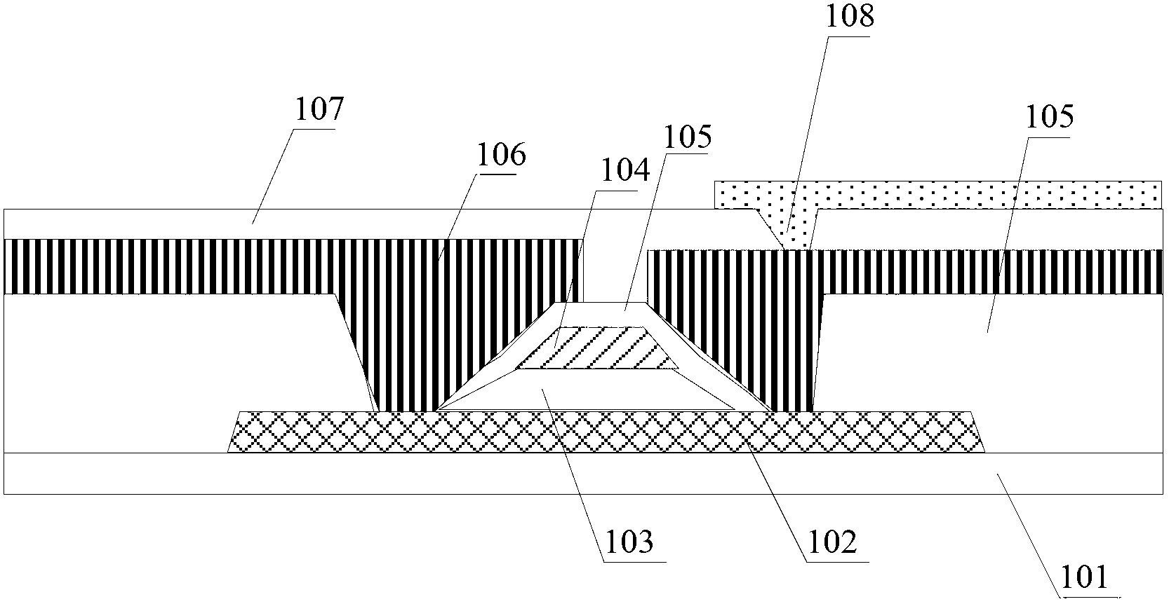
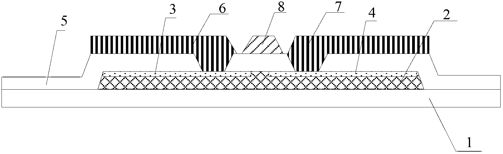
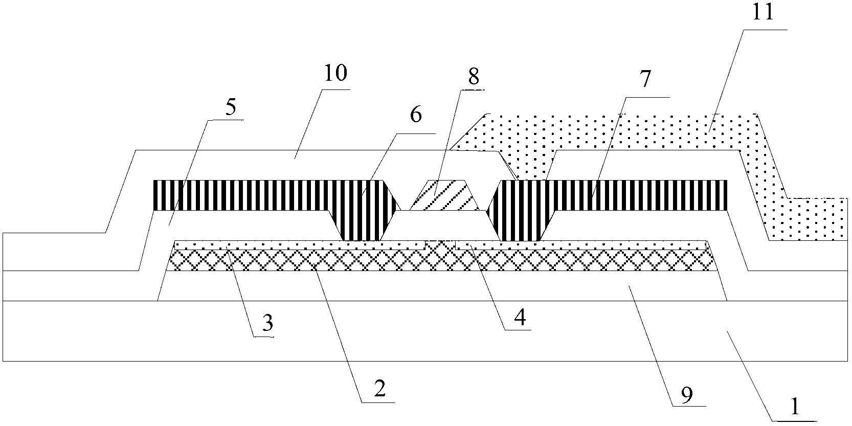
[0062] The embodiment of the present invention simplifies the structure of the TFT by fabricating the source, drain, and gate of the TFT in the same layer. The process of fabricating the TFT adopts the 5Mask process, which simplifies the TFT fabrication process. The active layer is provided with a first contact layer connected to the source and a second contact layer connected to the drain to avoid the generation of non-channel high-resistance regions, and to avoid the gate and source or gate and drain The formation of parasitic capacitance between them ensures the good electrical performance of the TFT.

[0063] The TFT provided by the embodiment of the present invention will be described in detail below with reference to the accompanying drawings.

[0064]...


PUM


Abstract

The invention discloses a thin film transistor (TFT) and a manufacturing method thereof, an array substrate and a display device. The invention aims to provide a TFT with simple structure and better performance. The thin film transistor provided by the invention comprises a substrate, wherein an active layer is formed on the substrate; a first contact layer and a second contact layer which are conductive are formed on the active layer; an etching barrier layer is formed on the first contact layer and the second contact layer; a source electrode connected with the first contact layer, a drain electrode connected with the second contact layer, and a grid electrode positioned between the source electrode and the drain electrode are formed on the etching barrier layer; and a protective layer is formed on the source electrode, the drain electrode and the grid electrode.

Description

technical field [0001] The invention relates to the field of display technology, in particular to a thin film transistor, a manufacturing method thereof, an array substrate and a display device. Background technique [0002] In the field of display technology, oxide thin film transistor (Oxide Thin Film Transistor, Oxide TFT) is compared with amorphous silicon TFT because of its higher carrier mobility (carrier mobility is about ten times that of amorphous silicon TFT). times), as well as high thermal and chemical stability, has become a research hotspot. The display device driven by oxide TFT can meet the requirements of large-size and high-resolution display devices, especially the requirements of the next-generation active matrix organic light emitting display device (Active Matrix Organic Light Emitting Device, AMOLED). The display field occupies an important position. [0003] The requirements for making Oxide TFT are relatively high. On the premise of ensuring the pr...

Claims


Application Information

Patent Timeline
IPC IPC(8): H01L29/786H01L27/12H01L21/336
CPCH01L27/1248H01L29/41733H01L29/45H01L29/78633H01L29/78693H01L29/7869H01L27/1225H01L29/66969H01L27/1262
Inventor 张立姜春生王东方陈海晶刘凤娟
Owner BOE TECH GRP CO LTD
Why Eureka
Try Eureka