
Manufacturing method of PN node of P-type pseudo-single crystal silicon solar cell

A manufacturing method and technology of quasi-single crystal silicon, applied in the direction of final product manufacturing, sustainable manufacturing/processing, circuits, etc. Performance and conversion efficiency and other issues, to achieve the effect of reducing the difference in battery square resistance and improving electrical performance and conversion efficiency

Active Publication Date: 2013-07-31
RENESOLA JIANGSU LTD
View PDF4 Cites 11 Cited by
  • Summary
  • Abstract
  • Description
  • Claims
  • Application Information

AI Technical Summary

Problems solved by technology

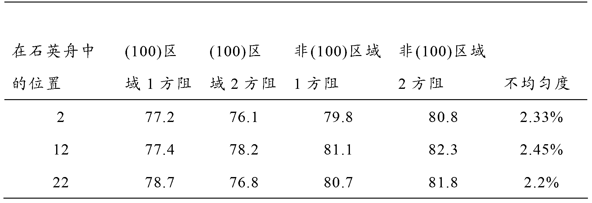
[0008] Although this method can complete the manufacturing process of the PN junction, the square resistance of the PN junction of the quasi-monocrystalline silicon solar cell manufactured by this method is quite different in the crystal direction (100) region and the non-(100) region. This will have a great impact on the subsequent sintering process, which is not conducive to the improvement of the electrical performance and conversion efficiency of quasi-monocrystalline silicon solar cells.

Method used


Image

  • Manufacturing method of PN node of P-type pseudo-single crystal silicon solar cell
  • Manufacturing method of PN node of P-type pseudo-single crystal silicon solar cell
  • Manufacturing method of PN node of P-type pseudo-single crystal silicon solar cell

Examples


Embodiment 1

[0038] Put a set of P-type quasi-monocrystalline silicon wafers after texturing and cleaning into the diffusion furnace. In this embodiment, a set of P-type quasi-monocrystalline silicon wafers is specifically 25 pieces, which are carried by a quartz boat. Quasi-monocrystalline silicon wafers are processed as follows:

[0039] Adjust the temperature in the diffusion furnace to 750°C (that is, the first temperature), and pretreat the P-type quasi-monocrystalline silicon wafers at a pressure of -50pa (first pressure). The processing time is preferably 5-10 minutes ;

[0040] Then increase the temperature to increase the temperature in the diffusion furnace to 800°C (the second temperature), and carry phosphorus oxychloride into the diffusion furnace by nitrogen at a pressure of -50pa, maintaining the flow rate of phosphorus oxychloride at 1L / min, the duration is 10 minutes;

[0041] Then lower the temperature, stop the introduction of phosphorus oxychloride, keep the temperature in ...

Embodiment 2

[0053] Put a set of P-type quasi-monocrystalline silicon wafers after texturing and cleaning into the diffusion furnace. In this embodiment, a set of P-type quasi-monocrystalline silicon wafers is specifically 25 pieces, which are carried by a quartz boat. Quasi-monocrystalline silicon wafers are processed as follows:

[0054] Adjust the temperature in the diffusion furnace to 750°C (ie the first temperature), and pretreat the P-type quasi-single crystal silicon wafers at a pressure of -100pa (first pressure). The processing time is preferably 5-10 minutes ;

[0055] Then increase the temperature to increase the temperature in the diffusion furnace to 750°C (the second temperature), and carry phosphorus oxychloride into the diffusion furnace by nitrogen at a pressure of -100 pa, keeping the flow rate of phosphorus oxychloride at 0.5 L / min, duration is 15 minutes;

[0056] Then lower the temperature, stop the introduction of phosphorus oxychloride, keep the temperature in the diffus...

Embodiment 3

[0068] Put a set of P-type quasi-monocrystalline silicon wafers after texturing and cleaning into the diffusion furnace. In this embodiment, a set of P-type quasi-monocrystalline silicon wafers is specifically 25 pieces, which are carried by a quartz boat. Quasi-monocrystalline silicon wafers are processed as follows:

[0069] Adjust the temperature in the diffusion furnace to 725°C (that is, the first temperature), and pretreat the P-type quasi-single crystal silicon wafers under a pressure of -75pa (first pressure). The processing time is preferably 5-10 minutes ;

[0070] Then increase the temperature to increase the temperature in the diffusion furnace to 775°C (the second temperature), and carry phosphorus oxychloride into the diffusion furnace by nitrogen at a pressure of -75pa, keeping the flow rate of phosphorus oxychloride at 0.75 L / min, duration is 12 minutes;

[0071] Then lower the temperature, stop the introduction of phosphorus oxychloride, keep the temperature in the...


PUM


Abstract

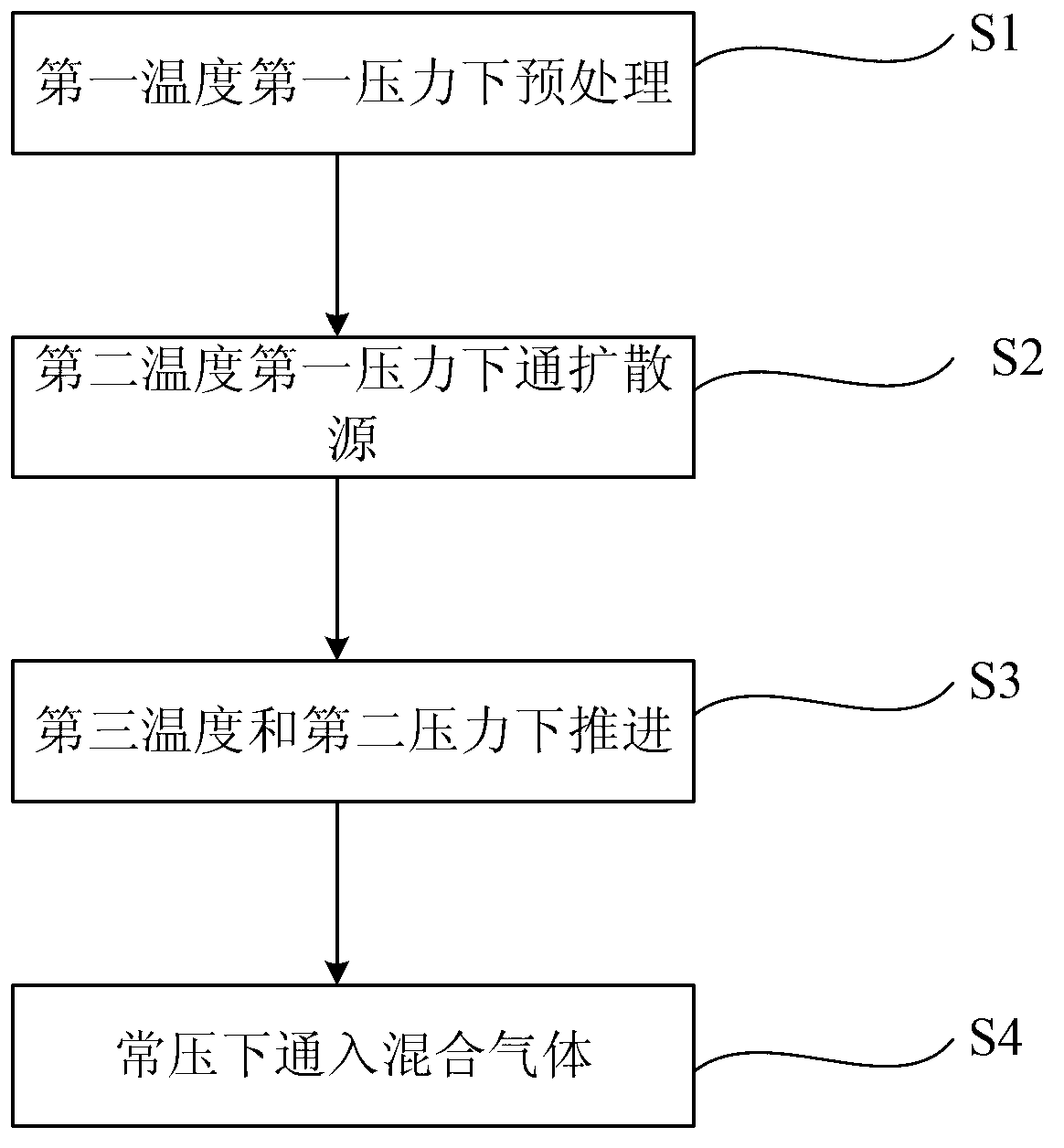
The invention discloses a manufacturing method of a PN node of a P-type pseudo-single crystal silicon solar cell. The method comprises the following steps sequentially carried out on a P-type pseudo-single crystal silicon in a reactor: pre-treating the P-type pseudo-single crystal silicon under a first temperature and a first pressure, wherein the first temperature is between 700 DEG C and 750 DEG C, and the first pressure is between -100pa and -50pa; introducing a diffusion source under a second temperature and the first pressure, wherein the second temperature is higher than the first temperature and not higher than 800 DEG C; propelling the diffusion source under a third temperature and a second pressure, wherein the third temperature is higher than 700 DEG C and lower than the second temperature, and the second pressure is between 100pa and 300pa; and introducing mixed gas of nitrogen and oxygen so as to finish the manufacture of PN nodes. By adopting the manufacturing method of the P-type pseudo-single crystal silicon solar cell, the difference between the cell sheet resistances of a crystal orientation region (100) and a non-crystal orientation region (100) can be effectively reduced, so that the subsequent sintering process is facilitated and the electrical property and the conversion efficiency of cells are improved.

Description

Technical field [0001] The invention relates to the technical field of solar cell manufacturing, in particular to a method for manufacturing a PN junction of a P-type quasi-monocrystalline silicon solar cell. Background technique [0002] The PN junction is the most important part of the solar cell, so the manufacturing process of the PN junction is also one of the most important links in the solar cell manufacturing process. The diffusion doping method is a common method for preparing the PN junction of the solar cell. The so-called diffusion doping method is Under high temperature conditions, specific impurities are used for diffusion, and the impurity atoms are doped into the silicon substrate to form a PN junction in a specific area. [0003] The so-called quasi-single-crystalline silicon is actually polycrystalline silicon with relatively ordered atomic arrangement. Its crystal orientation is more consistent. The crystal silicon has a higher grain boundary, and the atomic arra...

Claims


Application Information

Patent Timeline
IPC IPC(8): H01L31/18
CPCY02P70/50
Inventor 王立建
Owner RENESOLA JIANGSU LTD
Learn More