

Photomask with novel three-layer-film structure, and preparation method thereof
A technology of three-layer film and photomask, which is applied in the fields of chemical instruments and methods, photoplate making process of patterned surface, optics, etc., can solve the problem of inability to ensure etching time, etch rate, product storage period, and sodium ion precipitation Aggravation and other problems, to achieve the effect of clear etching lines, stable etching speed and good uniformity
- Summary
- Abstract
- Description
- Claims
- Application Information
AI Technical Summary
Problems solved by technology
Method used
Image


Examples
Embodiment 1
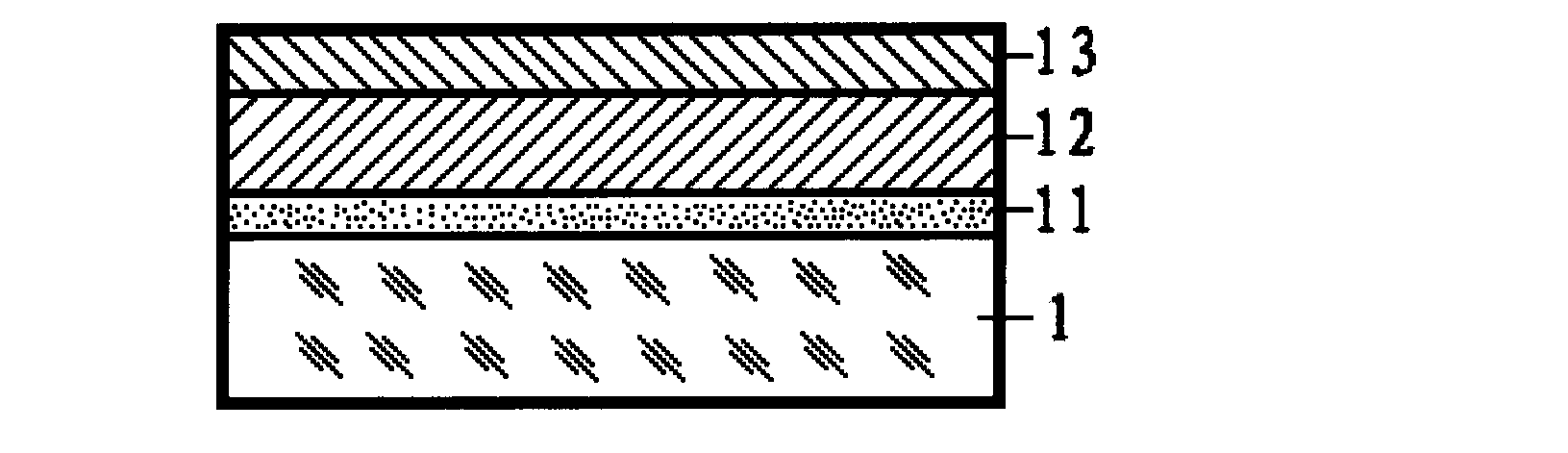
[0037] Such as figure 1The photomask of the most preferred new three-layer film structure of the present invention comprises glass substrate 1, chromium carbonitride barrier layer 11, chromium carbonitride light-shielding film layer 12, chromium carbonitride anti-reflection film Layer 13, the chromium carbonitride barrier layer 11, the chromium carbonitride light-shielding film layer 12, and the chromium carbonitride anti-reflection film layer 13 are sequentially plated on the glass substrate. The glass substrate 1 may be a soda-lime glass substrate, a quartz glass substrate, a borosilicate glass substrate or a corona glass substrate. The thickness of the chromium oxycarbonitride barrier layer 11 is The thickness of the chromium carbonitride light-shielding film layer 12 is The thickness of the chromium carbonitride anti-reflection film layer 13 is
[0038] Prepare the photomask of the most preferred new three-layer film structure of the present invention as follows:
...
Embodiment 2
[0047] Four different substrate glasses (soda-lime glass, quartz glass, borosilicate glass, and corona glass) were used to prepare 4 samples of the most preferred new three-layer film structure of the present invention, and the preparation method was carried out according to Example 1.
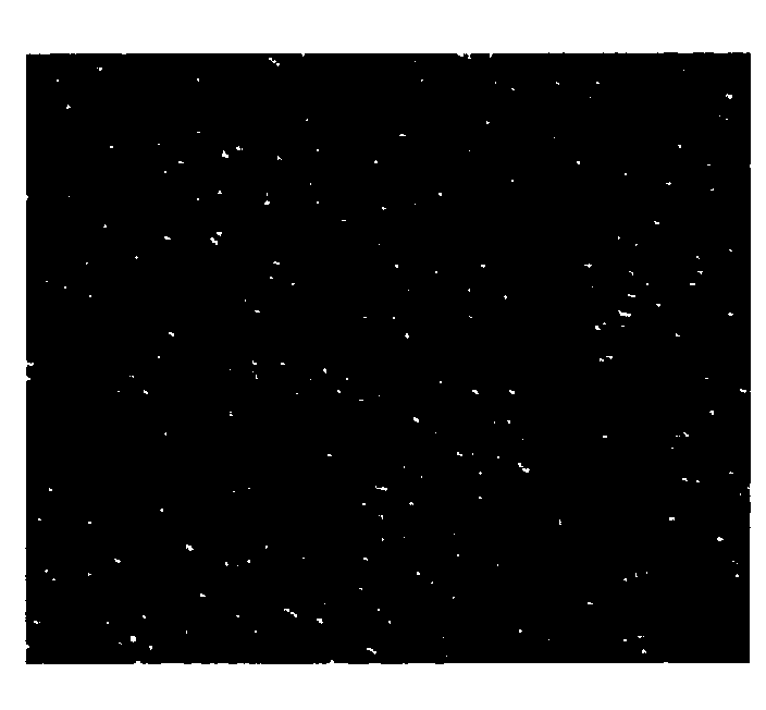
[0048] Put the above-mentioned coated sample glass into a clean oven, raise the temperature to 160°C and keep it warm for 1 hour, then cool it down to room temperature naturally. Then put the above samples into the following etching solution and soak for 15s (700g cerium ammonium nitrate + 150ml, 98% glacial acetic acid + 3500ml pure water), and then use a microscope to observe the pinholes one by one with a 500 times lens Condition.
[0049] The pinhole observation results are: 20 soda-lime glass, 0 quartz glass, 1 borosilicate glass, and 5 corona glass.
[0050] This example shows that the barrier layer of the present invention has different barrier effects on substrates made of different m...
PUM
| Property | Measurement | Unit |
|---|---|---|
| Etch rate | aaaaa | aaaaa |
Abstract
Description
Claims
Application Information