
Large-area nanometer imaging device and large-area nanometer imaging method

A nano-pattern, large-area technology, applied in micro-structure devices, manufacturing of micro-structure devices, photo-engraving process of pattern surface, etc. The effect of good graphic consistency, large embossed graphic area and good mold release performance

Active Publication Date: 2013-08-07
QINGDAO BONA PHOTOELECTRIC EQUIP
View PDF4 Cites 33 Cited by
  • Summary
  • Abstract
  • Description
  • Claims
  • Application Information

AI Technical Summary

Problems solved by technology

[0003] However, for various existing micro-nano manufacturing technologies (such as optical lithography, electron beam lithography, laser interference lithography, holographic lithography, etc.), the maximum patterning area is currently limited to a 12-inch wafer (300mm), and for The flatness of the substrate is demanding, especially facing challenging technical problems such as high production costs and low efficiency
In addition, the high-efficiency, low-cost large-area nanopatterning process Roll-to-roll nanoimprinting (Roll-to-roll NIL) is mainly aimed at large-area nanopatterning of flexible substrates, and is not suitable for patterning non-flat rigid substrates.
Traditional flat plate (flat plate, flat plate mold imprinting rigid substrate) nanoimprinting and roller type (rolling flat, roller mold imprinting rigid substrate) nanoimprinting face the following difficulties: (1) large area Uniform pressure (to ensure the consistency of imprinted patterns and residual layer thickness); (2) large-area conformal contact with non-flat substrates; (3) low efficiency, flat-panel nanoimprinting cannot achieve large-area imprinting and continuous Graphical, roller-type nano-imprint line contact curing takes a long time; (4) Large-area demoulding (even if flexible film molds and uncovered demoulding solutions are used, there are bubbles for large-area nano-patterning above 300 mm (5) Many problems such as short mold life and difficult mold manufacturing make it difficult to achieve nanopatterning of large-area non-flat rigid substrates larger than 12 inches
Therefore, none of the existing processes and methods can meet the requirements for large-scale patterned industrial-scale production of non-flat rigid substrates larger than 12 inches, which has severely restricted large-area functional surface nanostructures and nanostructured coatings. The application and promotion in high-performance glass, solar panels, flat panel display and other industries has become a bottleneck restricting the promotion and application of this technology

Method used


Image

  • Large-area nanometer imaging device and large-area nanometer imaging method
  • Large-area nanometer imaging device and large-area nanometer imaging method
  • Large-area nanometer imaging device and large-area nanometer imaging method

Examples


Embodiment Construction

[0032] The present invention will be further described below in conjunction with the accompanying drawings and embodiments.

[0033] The present invention takes the nano-patterning of glass as an embodiment, and manufactures a large-area structure on a coating on a glass substrate.

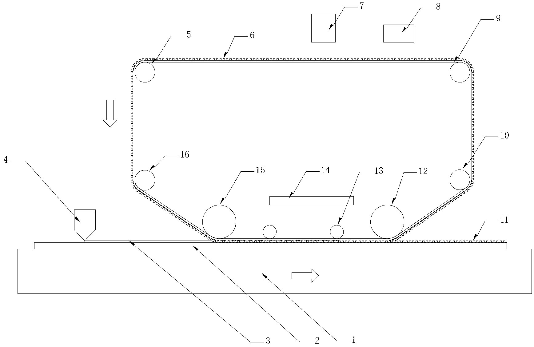
[0034] figure 1It is a schematic diagram of the structure of the large-area nano-patterning device of the present invention, which includes: a substrate 1, a substrate (glass) 2, a liquid imprinting material (transparent UV-curable polymer) 3, a coating device 4, and a mold feed Units 5 and 9, strip mold 6, release agent spraying unit 7, mold cleaning unit 8, mold guides 10 and 16, embossed features 11, stripping roller 12, auxiliary embossing unit 13, UV curing unit 14. Imprinting device 15. Wherein the substrate 2 is placed on the wafer table 1, and the liquid imprint material 3 is evenly coated on the upper surface of the substrate 2 by the coating device 4, and the belt-shaped mold 6 is woun...


PUM

PropertyMeasurementUnit
thicknessaaaaaaaaaa
thicknessaaaaaaaaaa

Abstract

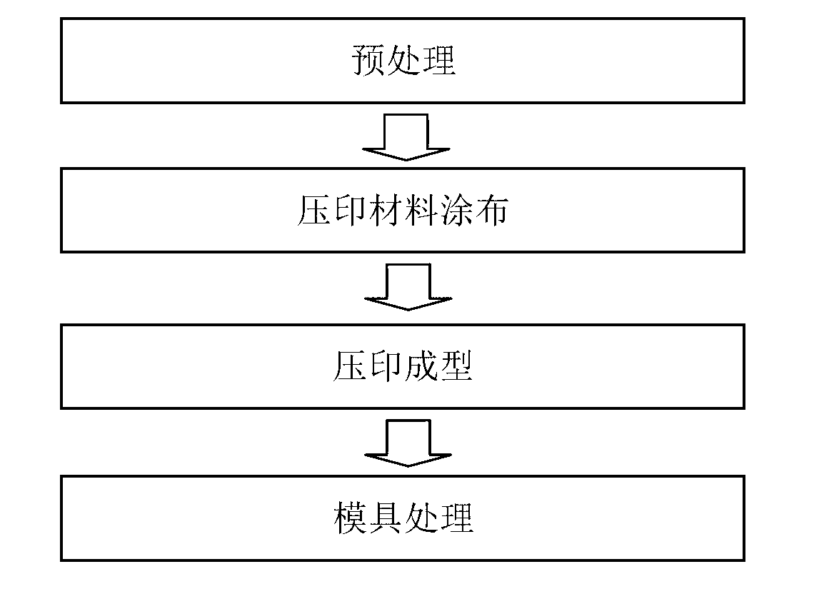
The invention discloses a large-area nanometer imaging device and a large-area nanometer imaging method. The device comprises a piece-supporting platform, a substrate, a coating device, mould feeding devices, a belt-shaped module, a release agent spraying device, a module cleaning device, an auxiliary impression device, an UV (Ultraviolet) solidifying device, an impression device and the like. The method for realizing large-area nanometer imaging based on the device comprises the following steps of: (1) pretreating; (2) coating an impression material; (3) performing impression molding; and (4) processing a mould. The large-area nanometer imaging device and the large-area nanometer imaging method, provided by the invention, have the advantages that a nanostructure on a non-smooth rigidity line with an oversized size is manufactured in an efficient and low-cost large-scale manner, an industrial-grade solution is provided for large-area nanometer imaging of a large-size rigidity substrate, and the large-area nanometer imaging device and the large-area nanometer imaging method are applied in industry large-scale manufacture such as high-performance glass, solar panels, panel displays, micro-optics devices and LEDs (light-emitting diodes).

Description

technical field [0001] The invention belongs to the technical field of micro-nano manufacturing, and in particular relates to a large-area nano-patterning device and method suitable for super-large rigid substrates. Background technique [0002] Large-area functional surface nanostructures and nanostructure coatings can greatly improve product performance and product quality, and have very broad and huge commercial application prospects. For example, moth-eye (Moth-Eyes) structure or nano-cone structure is produced on the glass surface or the transparent coating on it, and the glass has excellent anti-reflection, self-cleaning, anti-glare, anti-fog, high transparency and other properties. High-performance glass can be widely used in high-rise building glass curtain walls and automobile front windshields, solar panels, flat panel displays (TV screens, touch screens, notebook screens, smart phone screens, etc.), optical devices (camera lenses, microscope lenses, optical lens)...

Claims


Application Information

Patent Timeline
Patent Type & Authority Applications(China)
IPC IPC(8): G03F7/00B81C1/00
Inventor 兰红波
Owner QINGDAO BONA PHOTOELECTRIC EQUIP
Learn More