Erasable film variable-resistance memory unit adopting flexible paper base and preparation method thereof

A technology of storage unit and resistive variable memory, which is applied in the direction of electrical components, etc., can solve the problems of large number of transistors, low storage density, increased production cost, etc., and achieve the effects of wide application prospects, high deposition rate, and good resistive variable performance

Inactive Publication Date: 2013-08-14
FUDAN UNIV
View PDF4 Cites 4 Cited by
  • Summary
  • Abstract
  • Description
  • Claims
  • Application Information

AI Technical Summary

Problems solved by technology

Each has its advantages and disadvantages: the disadvantages of static random access memory devices are that a memory unit requires a large number of transistors, is expensive, and has low storage density; dynamic random access memory devices need to be continuously refreshed to save data when the power is turned on, and the data will be lost after power-off. will be lost; flash memory is the only memory that can retain data without power, but it is relatively slow
However, many of the raw materials are expensive metals, or require expensive and complicated equipment to prepare thin films, increasing production costs

Method used


Image

  • Erasable film variable-resistance memory unit adopting flexible paper base and preparation method thereof
  • Erasable film variable-resistance memory unit adopting flexible paper base and preparation method thereof
  • Erasable film variable-resistance memory unit adopting flexible paper base and preparation method thereof

Examples


Embodiment Construction

[0030] Specific embodiments of the present invention will be further described below through specific examples.

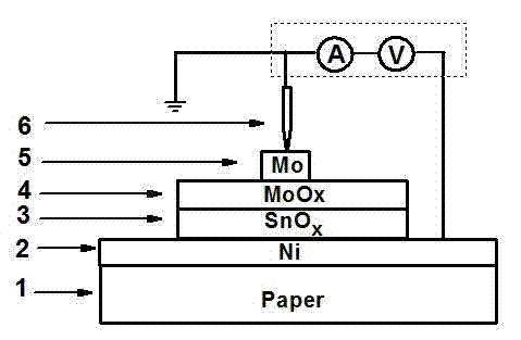
[0031] The metal Ni target is selected, and the vacuum of the reaction chamber is lowered to less than 3.0×10 before film deposition. -3 Pa, and then the Ar gas is passed into the reaction chamber through the variable gas guide valve, and the working pressure in the reaction chamber is controlled to be 2.0×10 -1Pa. The sputtering current and voltage were adjusted to 180 mA and 500 V, respectively, and the sputtering time was 20 minutes to form a metal nickel film on the ink paper substrate as the bottom electrode. Electrode square resistance is less than 10 ohms.

[0032] Select a metal tin target, and vacuum the reaction chamber to less than 3.0×10 before film deposition -3 Pa, the substrate is heated to 100°C, and then the O 2 and Ar gas are passed into the reaction chamber in turn, and the oxygen partial pressure in the reaction chamber is controlled to be...


PUM

PropertyMeasurementUnit
Thicknessaaaaaaaaaa
Thicknessaaaaaaaaaa

Abstract

The invention belongs to the technical field of nonvolatile memory devices, and particularly relates to an erasable film RRAM (resistive random access memory) memory unit. The memory unit is characterized in that a piece of flexible and bendable printing ink color printing paper is used as a substrate, a tin oxide film is used as a variable-resistance layer, and a molybdenum oxide film is used as an oxygen storage layer; and a specific structure comprises the printing ink color printing paper substrate, a metallic nickel film serving as a bottom electrode, the tin oxide film, the molybdenum oxide film and a metallic molybdenum film serving as a top electrode in sequence. According to the invention, a direct current magnetron sputtering technology is used at the low temperature (subzero 100 DEG C), and the metallic nickel film, the tin oxide film, the molybdenum oxide film and the metallic molybdenum film are prepared on the substrate sequentially. The variable-resistance memory unit prepared by the invention has the characteristics of good bending durability and the like, and has a wide application prospect in the fields of nonvolatile memory and flexible electron devices.

Description

technical field [0001] The invention belongs to the technical field of non-volatile storage devices, and in particular relates to a rewritable thin-film resistive storage unit and a preparation method thereof. Background technique [0002] The mechanism of Resistive Random Access Memory (RRAM) is that an external electric field triggers a reversible resistance transition effect, that is, under the action of an applied voltage, the resistance of the device is in a low resistance state (“0”) and a high resistance state (“1”) ”), and the resulting resistance can be maintained after the external electric field is removed. Based on this effect, the scientific community has proposed a new concept of non-volatile memory - resistive random access memory 。 The ultimate goal of RRAM technology is to change multiple memory devices contained in an existing single electronic product into a single memory unit. In the next few years, it will be more widely used in circuit chips with vari...

Claims


Application Information

Patent Timeline
IPC IPC(8): H01L45/00
Inventor 张群刘宝营
Owner FUDAN UNIV
Why Eureka
Try Eureka