TSV front end portion interconnection process

A process and substrate surface technology, applied in electrical components, semiconductor/solid-state device manufacturing, circuits, etc., can solve the problems of large film stress, increased process difficulty, easy delamination or cracks between the insulating layer and the substrate, and achieve improved quality and Reliability, the effect of reducing difficulty

Active Publication Date: 2013-09-04
NAT CENT FOR ADVANCED PACKAGING CO LTD
View PDF3 Cites 6 Cited by
  • Summary
  • Abstract
  • Description
  • Claims
  • Application Information

AI Technical Summary

Problems solved by technology

[0005] In the current isotropic dry etching process of TSV, there will be protrusions at the edge of the TSV hole. When making SiO 2 When the insulating layer, seed layer and copper are filled, a multi-layer structure "stress concentration" area will be formed, which will cause easy delamination or cracks between the insulating layer and the substrate here, seriously affecting the quality and reliability of TSV, and the current The process cannot eliminate the influence of the stress concentration area;
[0006] In order to meet the TSV hole insulation layer (SiO 2 ) coverage, when deposited, the surface insulating layer is generally very thick, which will produce a large SiO 2 Thin film stress, which will also affect the quality and reliability of TSV;
[0007] In addition, when the CMP process is performed, the polishing accuracy needs to be controlled to retain a certain thickness of the insulating layer on the silicon-based surface, which increases the difficulty of the process

Method used


Image

  • TSV front end portion interconnection process
  • TSV front end portion interconnection process
  • TSV front end portion interconnection process

Examples


Embodiment Construction

[0037] The present invention reduces or removes the stress concentration area of ​​the TSV conductive column, reduces the possibility of delamination or cracks between the insulating layer and the substrate due to stress; It will highlight the defects of this existing process and realize the interconnection between the TSV conductive pillar and the redistribution layer metal.

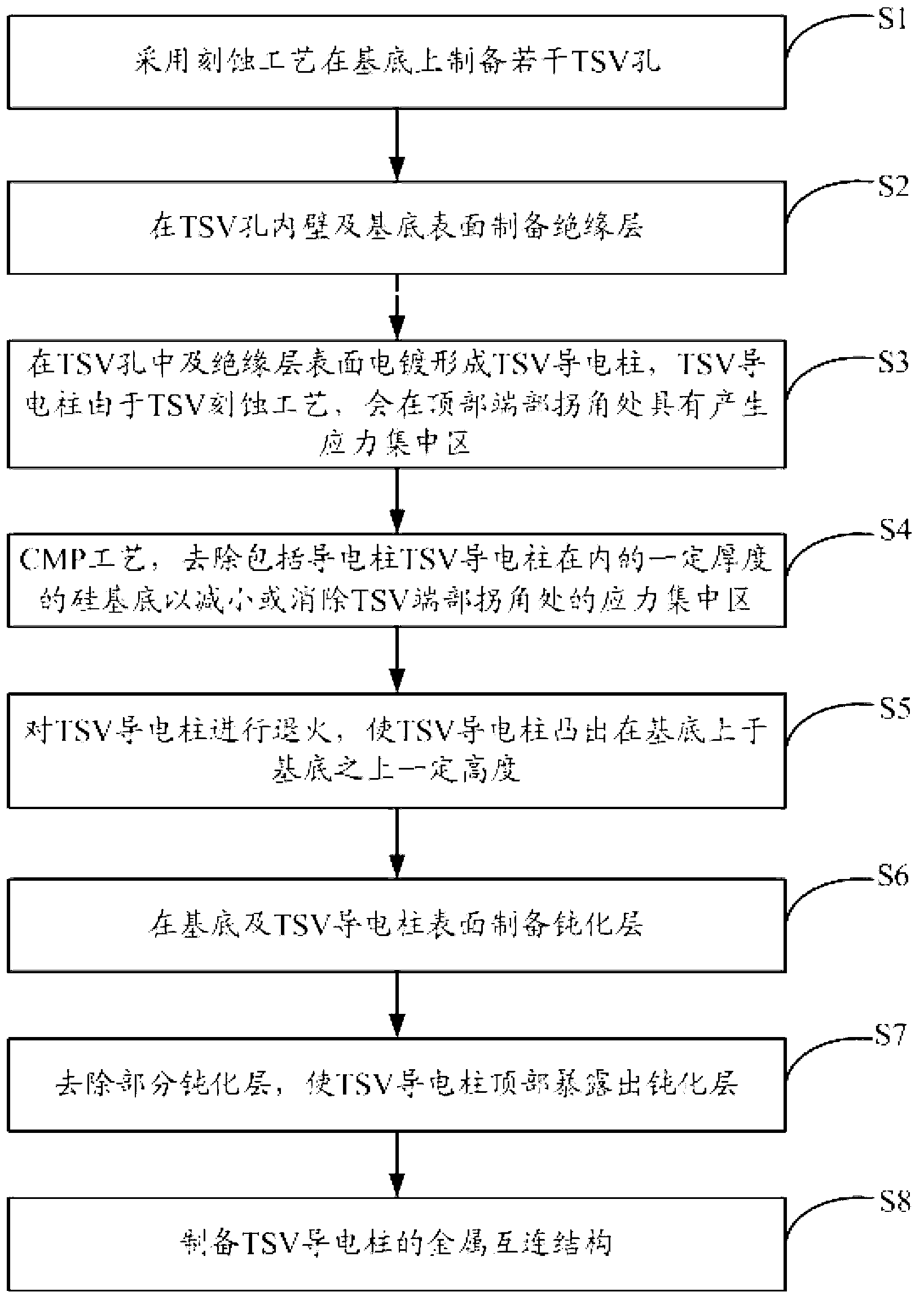
[0038] Specifically, such as figure 1 As shown, a TSV front end interconnection process disclosed in the present invention includes the following steps:

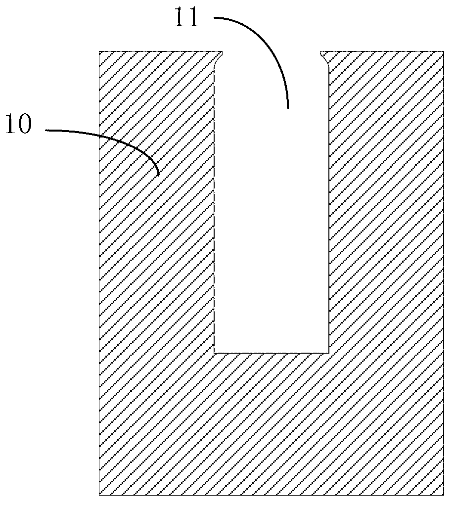
[0039] S1, using an etching process to prepare a number of TSV holes on the substrate;

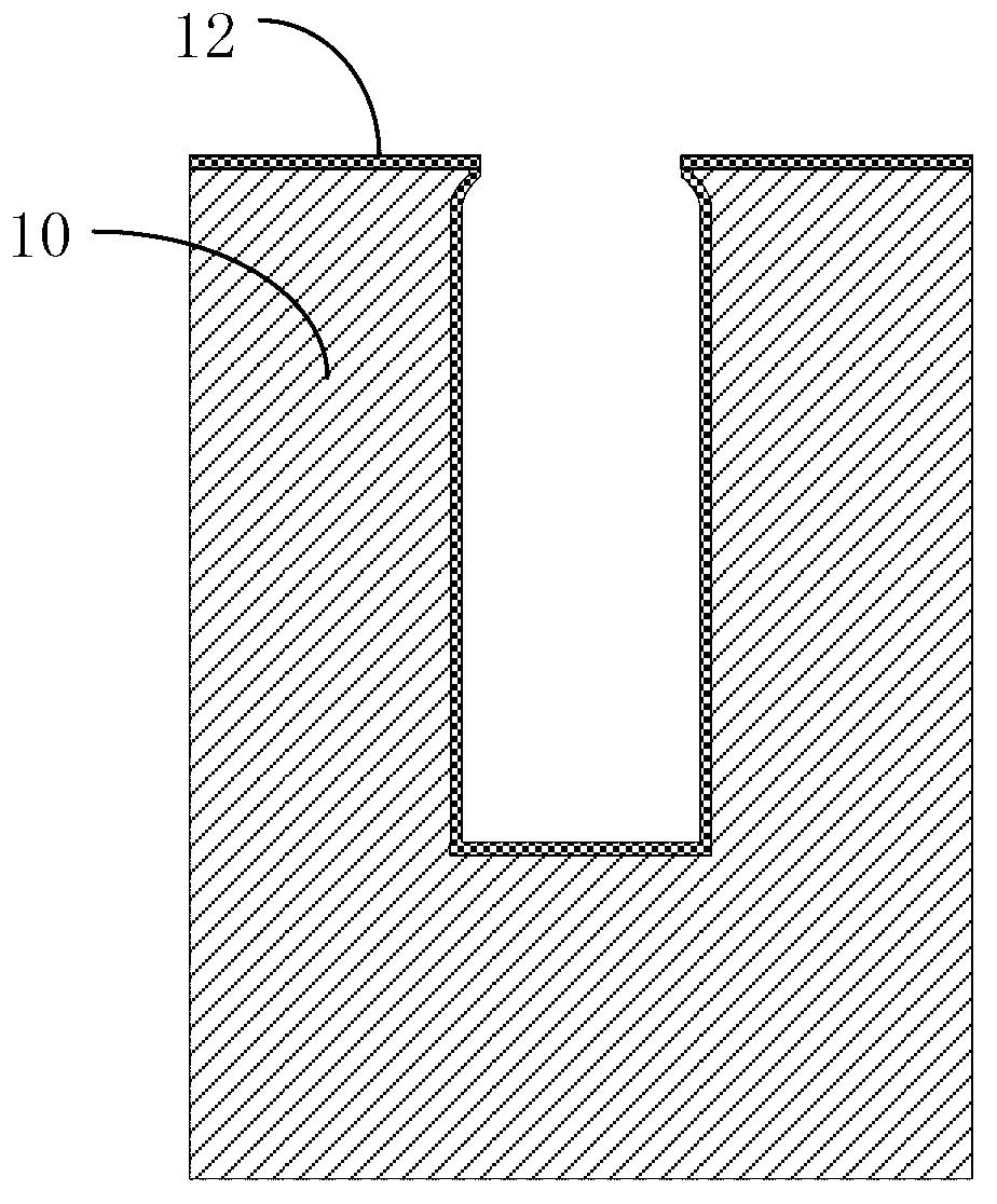
[0040] S2, preparing an insulating layer on the inner wall of the TSV hole and the surface of the substrate;

[0041] S3, forming TSV conductive columns in the TSV holes and on the surface of the insulating layer by electroplating, and the TSV conductive columns will generate stress concentration areas at the corners of the ends due to the TSV etching process; ...


PUM


Abstract

The invention discloses a TSV front end portion interconnection process. The process includes preparing a plurality of TSV holes in a substrate by means of the etching technology; preparing insulating layers on the inner walls of the TSV holes and on the surface of the substrate; forming TSV conductive columns in the TSV holes and on the surfaces of the insulating layers through electroplating; eliminating a silicon substrate with a certain thickness including the TSV conductive columns through the CMP technology; carrying out annealing on the TSV conductive columns so that the TSV conductive columns can extrude out of the substrate at a certain height; preparing passivation layers on the substrate and the surfaces of the TSV conductive columns, and eliminating a part of the passivation layers so that the tops of the TSV conductive columns can be exposed out of the passivation layers; preparing a metal interconnection structure of the TSV conductive columns. The TSV front end portion interconnection process reduces or eliminates stress concentration areas at corners of the end portions of the TSV conductive columns, reduces probability that due to stress, delamination and cracks are formed between the insulating layers and the substrate, and meanwhile achieves interconnection of the TSV conductive columns and redistribution layer metal through use of the defect that after the TSV conductive columns are electroplated and processed through annealing, the TSV conductive columns will extrude.

Description

technical field [0001] The invention relates to the field of semiconductor integration technology or three-dimensional integration technology, in particular to a TSV front end interconnection process. Background technique [0002] With the continuous advancement of microelectronics technology, the feature size of integrated circuits has been continuously reduced and the interconnection density has been continuously increased. At the same time, users' requirements for high performance and low power consumption continue to increase. In this case, the way to improve the performance by further reducing the line width of the interconnection is limited by the physical characteristics of the material and the equipment process, and the resistance-capacitance (RC) delay of the two-dimensional interconnection gradually becomes the limit to improve the performance of the semiconductor chip. bottleneck. The Through Silicon Via (TSV) process can realize direct three-dimensional interco...

Claims


Application Information

Patent Timeline
Patent Type & Authority Applications(China)
IPC IPC(8): H01L21/768
CPCH01L21/76898
Inventor 戴风伟于大全
Owner NAT CENT FOR ADVANCED PACKAGING CO LTD
Why Eureka
Try Eureka