TFT-LCD (thin film transistor-liquid crystal display) array panel structure and production method thereof

A technology of array panel and manufacturing method, which is applied in the field of TFT-LCD array panel structure and its manufacturing, can solve the problems of reducing product yield and production cost, and achieve the effects of reducing production cost, reducing electrode corrosion, and reducing line resistance

Active Publication Date: 2013-09-04
CHENGDU TIANMA MICROELECTRONICS
View PDF3 Cites 10 Cited by
  • Summary
  • Abstract
  • Description
  • Claims
  • Application Information

AI Technical Summary

Problems solved by technology

[0007] During the manufacturing process of the above-mentioned TFT-LCD array panel 5mask, processes such as transmission, cleaning, and stripping will cause a large amount of electrostatic charge to accumulate on the surface of the glass substrate, between the gate and the source / drain, and between the source / drain and the pixel electrode. When the voltage difference between them is too large, a discharge phenomenon will occur, which is generally called an ESD phenomenon. The ESD phenomenon will cause a source-gate short circuit (DGS), a source and common electrode line short circuit (DCS), and a short circuit between data lines ( DDS), gate open circuit, data line short circuit and other electrostatic damage, resulting in various forms of line defects (Line defect) that cannot be repaired by subsequent processes, seriously reducing product yield and production costs

Method used


Image

  • TFT-LCD (thin film transistor-liquid crystal display) array panel structure and production method thereof
  • TFT-LCD (thin film transistor-liquid crystal display) array panel structure and production method thereof
  • TFT-LCD (thin film transistor-liquid crystal display) array panel structure and production method thereof

Examples


Embodiment 1

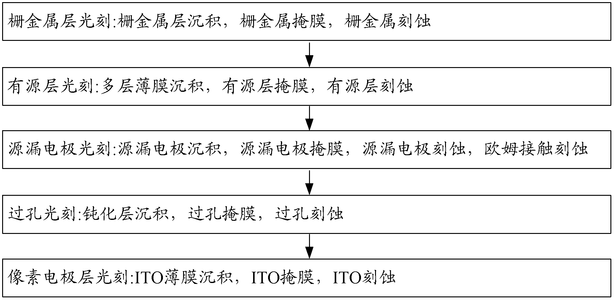
[0038] Such as figure 2 As shown, the present embodiment provides a manufacturing method of a TFT-LCD panel, comprising the following steps:

[0039] Gate metal layer photolithography: deposit a gate metal layer on the substrate and etch through a gate metal mask to form gate lines and gate electrodes;

[0040]Active layer photolithography: sequentially depositing a gate insulating layer, a semiconductor layer and an ohmic contact layer on the substrate, and sequentially etching the ohmic contact layer, semiconductor layer and gate insulating layer through a semi-transparent mask to form an island-shaped active layer (or silicon island) and expose part of the gate line;

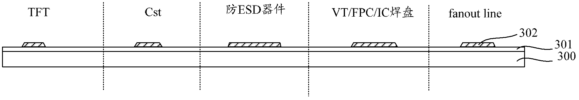
[0041] S / D photolithography: Deposit source / drain metal layers on the substrate, form source / drain and anti-ESD device base through source / drain mask etching, and the anti-ESD device base includes gate lines , exposing a gate insulating layer, a semiconductor layer, an ohmic contact layer of a part of the ...

Embodiment 2

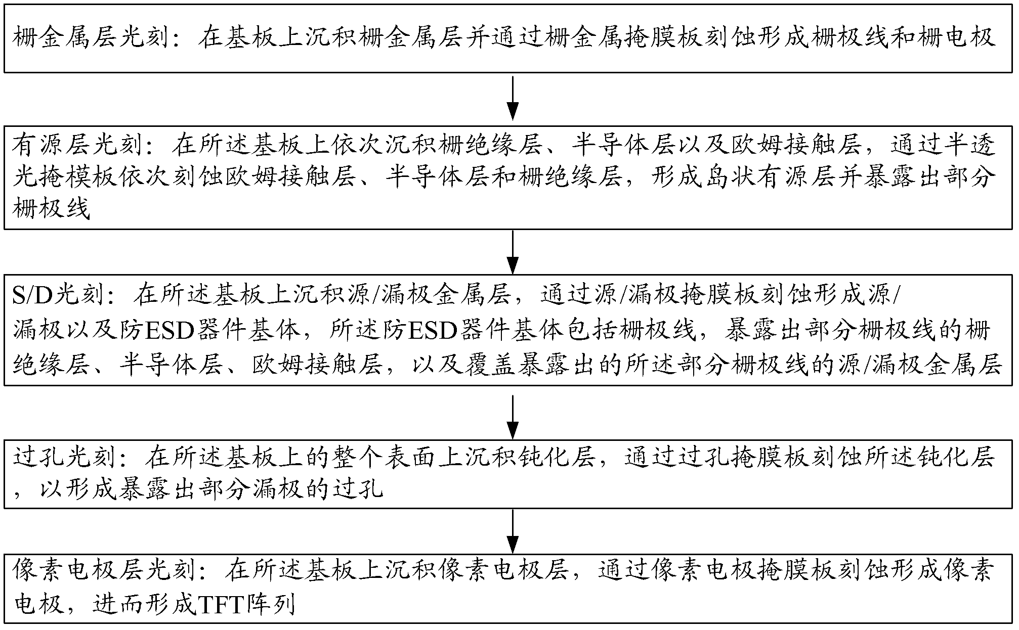
[0059] Such as Figure 5 As shown, the present embodiment provides a manufacturing method of a TFT-LCD panel, comprising the following steps:

[0060] Gate metal layer photolithography: deposit a gate metal layer on the substrate and etch through a gate metal mask to form gate lines and gate electrodes;

[0061] Active layer photolithography: sequentially depositing a gate insulating layer, a semiconductor layer, and an ohmic contact layer on the substrate, and sequentially etching the ohmic contact layer, semiconductor layer, and gate insulating layer through an active layer mask to expose part of the gate Wire;

[0062] S / D photolithography: Deposit the source / drain metal layer on the substrate, etch the source / drain metal layer, ohmic contact layer and exposed part of the gate line through the source / drain mask to form Source / drain and anti-ESD device substrate, the anti-ESD device substrate includes a gate line, a gate insulating layer that exposes a part of the gate lin...


PUM


Abstract

The invention provides a TFT-LCD (thin film transistor-liquid crystal display) array panel structure and a production method thereof. An anti-ESD (anti-electrostatic discharge) element of which a gate metal layer is in direct contact with a source/drain metal layer is produced outside a TFT array in order to prevent each process station after source/drain metal deposition from being injured by static electricity, so that the product percent of pass can be increased; meanwhile, by correspondingly changing active mask, silicon islands are formed in the process of via-hole mask, consequently, the process steps are simplified, and the production cost is reduced; meanwhile, by correspondingly changing gate mask, active mask and source/drain mask, the gate metal is covered by the source/drain metal in the area of a VT/FPC/IC pad, consequently, the electrode corrosion of the gate metal layer can be reduced, and in the extending area of a fanout line, the line resistance can be decreased; and furthermore, before the deposition of the gate metal layer, a silicon nitride layer is first formed, so that the injuries of a substrate caused by dry etch can be reduced.

Description

technical field [0001] The invention relates to the technical field of TFT-LCD manufacturing, in particular to a TFT-LCD array panel structure and a manufacturing method thereof. Background technique [0002] TFT-LCD (Thin film transistor liquid crystal display, Thin film transistor liquid crystal display) is a kind of liquid crystal display, which uses thin film transistor technology to improve image quality, and is widely used in TVs, flat panel displays and projectors. [0003] TFT-LCD is composed of three core components: display screen, backlight source and driving circuit. Simply put, a TFT-LCD display can be regarded as a layer of liquid crystal sandwiched between two glass substrates. The upper glass substrate has a color filter film (Color Filter), while the lower glass is embedded with TFT transistors. Polarizers are pasted on the outer sides of the upper and lower glass substrates respectively. When the current passes through the transistor, the electric field c...

Claims


Application Information

Patent Timeline
Patent Type & Authority Applications(China)
IPC IPC(8): H01L21/77H01L27/12G02F1/1368
Inventor 曾国波吴勃扈映茹黄贤军
Owner CHENGDU TIANMA MICROELECTRONICS
Why Eureka
Try Eureka