Planar power mos devices

A MOS device, planar technology, applied in the direction of semiconductor devices, electrical components, circuits, etc., can solve the problems of large layout area and volume reduction, and achieve the effect of increasing design space, reducing power consumption, and increasing gate width

Active Publication Date: 2016-01-27
SUZHOU VOCATIONAL UNIV
View PDF4 Cites 0 Cited by
  • Summary
  • Abstract
  • Description
  • Claims
  • Application Information

AI Technical Summary

Problems solved by technology

[0003] With the development of device miniaturization, the existing LDMOS design occupies a large layout area, which is not conducive to its integration with other functional devices to further reduce the volume and expand the application range. Therefore, how to design a device that can effectively reduce the current Some LDMOS occupy the surface area of ​​the silicon wafer and can further improve the performance of the device, becoming a technical obstacle

Method used


Image

  • Planar power mos devices
  • Planar power mos devices
  • Planar power mos devices

Examples


Embodiment 1

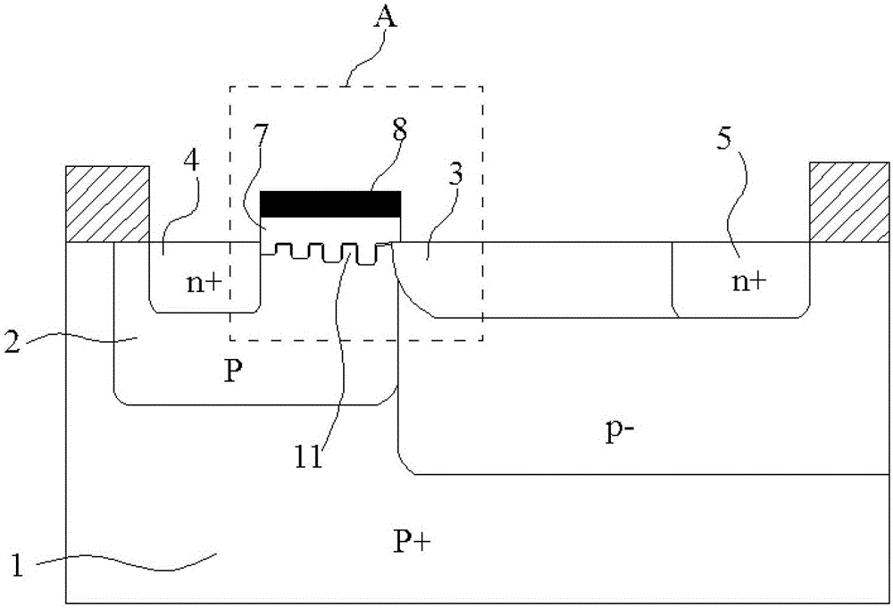
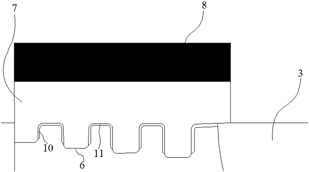
[0018] Embodiment 1: A planar power MOS device, comprising: a P-type well layer 2 and an N-type lightly doped layer 3 located in a P-type substrate layer 1, and the P-type well layer 2 and the N-type lightly doped layer Layers 3 are adjacent in the horizontal direction to form a PN junction, a source region 4 is located in the P-type well layer 2, a drain region 5 is located in the substrate layer 1, and a drain region 5 is located in the source region 4 and the N-type well layer. A gate oxide layer 7 is provided above the P-type well layer 2 in the area between the lightly doped layers 3, and a gate region 8 is provided above the gate oxide layer 7; the source region 4 and the N-type lightly doped layer 3 There are at least two grooves between and on the upper part of the P-type well layer 2, the etching depth of the grooves near the source region 4 is smaller than the etching depth of the grooves near the N-type lightly doped layer 3, and several of the grooves are The etchi...

Embodiment 2

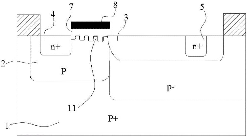
[0023] Embodiment 2: A kind of planar power MOS device, comprising: the P-type well layer 2 and the N-type lightly doped layer 3 in the P-type substrate layer 1, the P-type well layer 2 and the N-type lightly doped layer Layers 3 are adjacent in the horizontal direction to form a PN junction, a source region 4 is located in the P-type well layer 2, a drain region 5 is located in the substrate layer 1, and a drain region 5 is located in the source region 4 and the N-type well layer. A gate oxide layer 7 is provided above the P-type well layer 2 in the area between the lightly doped layers 3, and a gate region 8 is provided above the gate oxide layer 7; the source region 4 and the N-type lightly doped layer 3 There are at least two grooves between and on the upper part of the P-type well layer 2, the etching depth of the grooves near the source region 4 is smaller than the etching depth of the grooves near the N-type lightly doped layer 3, and several of the grooves are The etch...


PUM


Abstract

The invention discloses a planar power metal oxide semiconductor (MOS) device, which comprises a P-type trap layer positioned in a P-type substrate layer and an N-type lightly doped layer, wherein the P-type trap layer and the N-type lightly doped layer are adjacent in the horizontal direction to form a PN junction; a source region is positioned in the P-type trap layer; a drain region is positioned in the substrate layer; a gate-oxide layer is arranged on the P-type trap layer positioned between the source region and the N-type lightly doped layer; and a gate region is arranged on the gate-oxide layer. The planar power MOS device is characterized in that at least two grooves are formed between the source region and the N-type lightly doped layer and on the upper part of the P-type trap layer; the etching depth of the groove close to the source region is smaller than that of the groove close to the N-type lightly doped layer; and the etching depth of the plurality of grooves is increased sequentially from the source region to the N-type lightly doped layer. Therefore, breakdown voltage resistance is improved, the specific on-resistance of the device is reduced, the response time and frequency characteristic are improved, the whole performance is improved, and the size is reduced.

Description

technical field [0001] The invention relates to a MOS device, in particular to a planar power MOS device. Background technique [0002] Metal oxide power MOS semiconductor devices, with the rapid development of the semiconductor industry, power electronics technology represented by high-power semiconductor devices has developed rapidly, and its application fields have continued to expand, such as the control of AC motors and printer drive circuits. Among various power devices today, the laterally diffused MOS semiconductor device LDMOS has a high operating voltage and a relatively simple process, so LDMOS has broad development prospects. In the design of LDMOS devices, the breakdown voltage and on-resistance have always been the main goals that people pay attention to when designing such devices. The thickness of the epitaxial layer, doping concentration, and the length of the drift region are the most important parameters of LDMOS. The breakdown voltage can be increased by...

Claims


Application Information

Patent Timeline
Patent Type & Authority Patents(China)
IPC IPC(8): H01L29/78H01L29/10
CPCH01L29/1037H01L29/42368H01L29/7835
Inventor 陈伟元
Owner SUZHOU VOCATIONAL UNIV
Why Eureka
Try Eureka