

Single-layered positive photoresist photoetching method applied to metal stripping
A positive photoresist, metal stripping technology, applied in microlithography exposure equipment, optics, optomechanical equipment and other directions, can solve the problem of metal deposition on the side wall that cannot be completely eliminated, achieve small pattern stripping process, low baking temperature , The effect of helping metal stripping
- Summary
- Abstract
- Description
- Claims
- Application Information
AI Technical Summary
Problems solved by technology
Method used
Image

Examples
Embodiment 1
[0027] A Ti / Pt / Au / Ti (600nm) metal layer is fabricated on a semiconductor substrate by using a single-layer positive photoresist photolithography process. The positive photoresist is AZ7908 positive photoresist from AZ Electronic Materials, and the developer is a positive photoresist developer containing 2.38% TMAH (tetramethylammonium hydroxide).
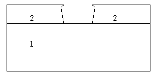
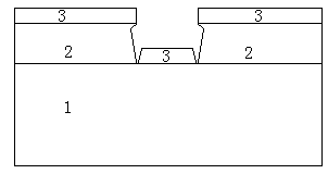
[0028] Its implementation steps: 1) Coating 7908 photoresist layer 2 on semiconductor substrate 1, 2) After developer treatment, exposure, and normal development, the formation of such as Figure 2A As shown in the figure, 3) Evaporation deposit metal layer 3 to semiconductor substrate 1, 7908 photoresist layer 2, such as Figure 2B As shown, 4) After stripping and removing the photoresist 2 and the metal layer 3 on it, the following Figure 2C The metal layer 3 shown.
[0029] The photolithography process used is: (1) The substrate is treated with dilute hydrochloric acid; (2) Glue coating, the thickness of the glue is 0.9μm; (3...
Embodiment 2
[0033] A Ni (150nm) metal layer was fabricated on a semiconductor substrate using a single-layer positive photoresist photolithography process. The positive photoresist is AZ7908 positive photoresist from AZ Electronic Materials, and the developer is a positive photoresist developer containing 2.38% TMAH (tetramethylammonium hydroxide).
[0034] Its implementation steps: 1) Coating 7908 photoresist layer 2 on the semiconductor substrate 1, 2) Forming a pattern after developer treatment, exposure, and normal development, 3) Evaporating and depositing the metal layer 3 on the semiconductor substrate 1, 7908 photolithography The adhesive layers 2, 4) are stripped to remove the photoresist 2 and the metal layer 3 thereon.
[0035] The photolithography process used is: (1) The substrate is treated with dilute hydrochloric acid; (2) Glue coating, the thickness of the glue is 0.9 μm; (3) Baking treatment after coating: temperature 90 ° C, time 60 seconds; (4) Containing 2.38% TMAH p...
Embodiment 3
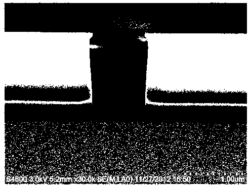
[0040]Change the exposure focal length from 0.0 to 1.0 to get a more prominent olecranon, which is good for Ni stripping. The final stripped metal has good morphology, such as Figure 6 shown.
PUM
| Property | Measurement | Unit |
|---|---|---|
| Thickness | aaaaa | aaaaa |
| Thickness | aaaaa | aaaaa |
| Thickness | aaaaa | aaaaa |
Abstract
Description
Claims
Application Information