Method for preferentially growing metallic single-walled carbon nanotube by using non-metallic silicon oxide as catalyst
A technology of single-walled carbon nanotubes and catalysts, which is applied in the fields of carbon nanotubes, non-metallic elements, chemical instruments and methods, etc., can solve the problem that metallic single-walled carbon nanotubes are difficult to selectively prepare, particle size is difficult to control, The structure is unstable at high temperature and other problems, which achieves good industrial application prospects, simple and easy-to-control processes, and wide applicability.
- Summary
- Abstract
- Description
- Claims
- Application Information
AI Technical Summary
Problems solved by technology
Method used
Image
Examples
Embodiment 1
[0043] Embodiment 1. Rapid heating mode
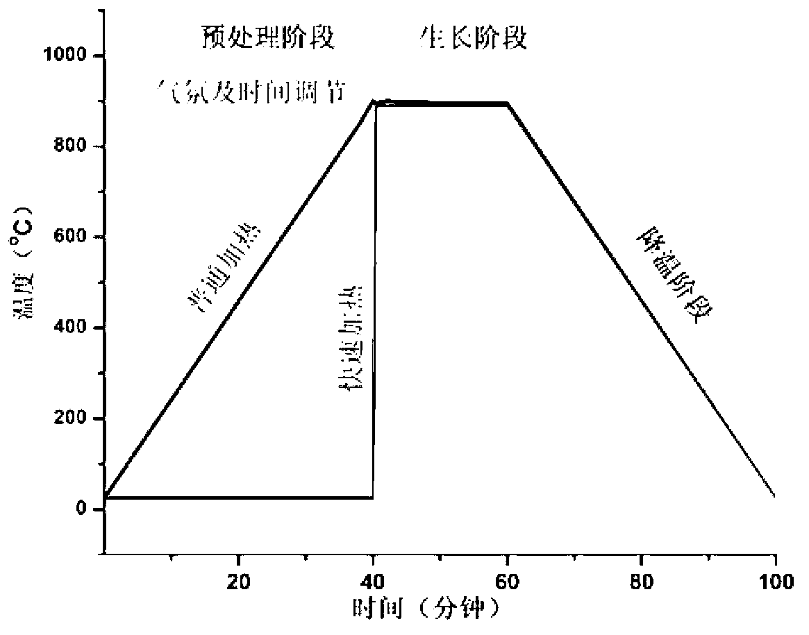
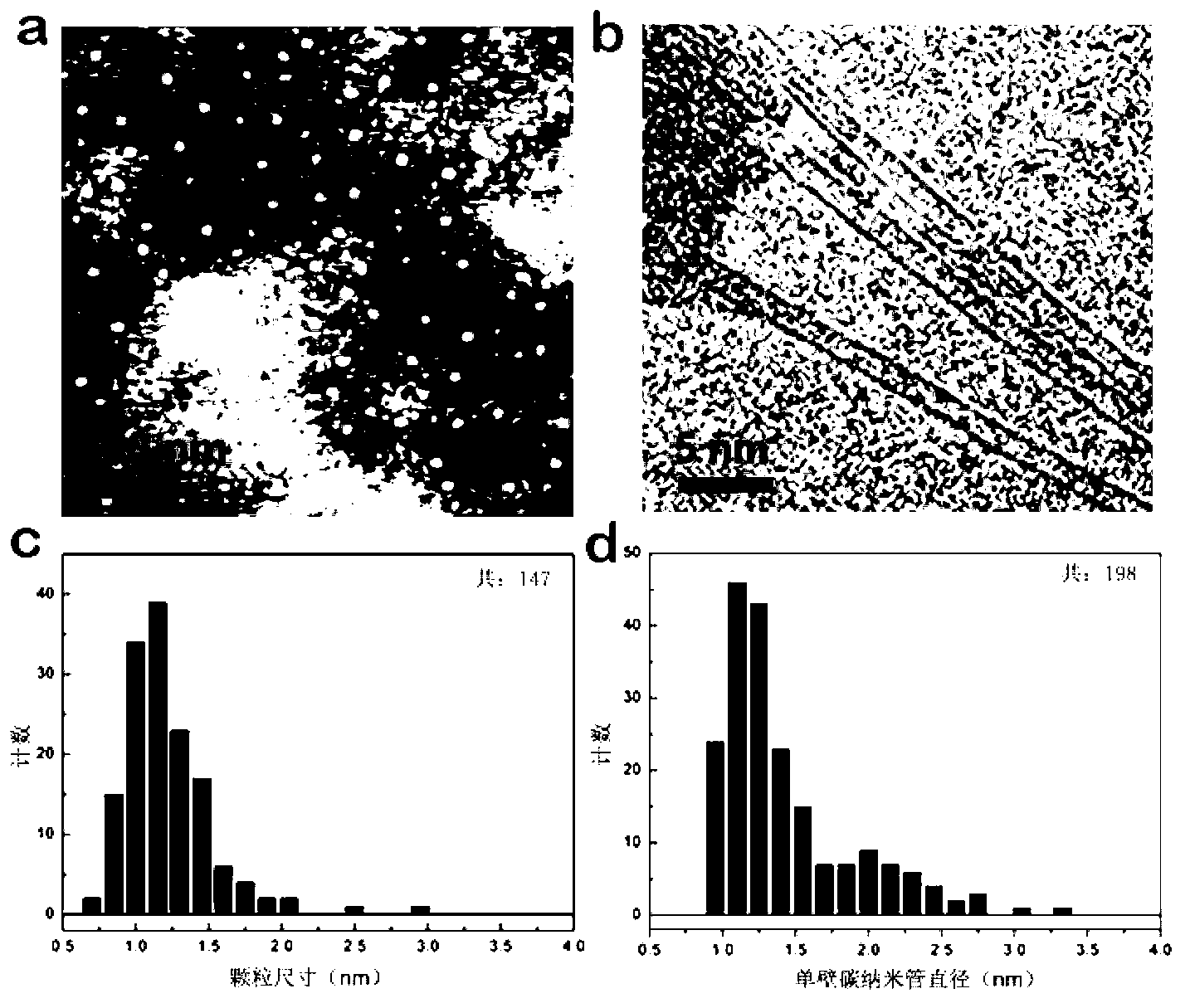
[0044] (1) A silicon wafer with a 55nm silicon oxide nanocatalyst layer deposited by Ar ion beam physical deposition method (the surface of the silicon wafer has a 300nm thermal oxide layer, and a silicon oxide nanolayer is deposited on the surface of the thermal oxide layer), and rapidly heated in an air atmosphere To 900°C, the rapid heating method refers to pushing the silicon wafer substrate containing the catalyst layer directly from room temperature to the center of the chemical vapor deposition furnace, and the center of the chemical vapor deposition furnace has reached the target temperature (900°C) suitable for the growth of single-walled carbon nanotubes; When the temperature of the substrate of the silicon wafer containing the catalyst layer reaches 900°C, anneal in air for 10 minutes, then evacuate the air in the furnace, introduce argon to restore normal pressure and maintain 400 sccm argon for 1.5 minutes, and then re-intr...
Embodiment 2
[0047] Embodiment 2. Semi-rapid heating mode
[0048] (1) A silicon wafer with a 30nm silicon oxide nanocatalyst layer deposited by Ar ion beam physical deposition method (the surface of the silicon wafer has an 80nm thermal oxide layer, and a silicon oxide nanolayer is deposited on the surface of the thermal oxide layer), and is rapidly heated in an air atmosphere to 850°C, the semi-rapid heating method refers to directly pushing the silicon wafer substrate containing the catalyst layer from room temperature to a chemical vapor deposition furnace with a temperature of 850°C; when the temperature of the silicon wafer substrate containing the catalyst layer reaches 850°C, in air Medium annealing for 3 minutes, then evacuate the air in the furnace, introduce argon gas to restore normal pressure and raise the temperature to 900°C within 2 minutes under 400 sccm argon gas, and keep the constant temperature protection at this temperature for 3 minutes; Certain ethanol vapor (argon ...
PUM
| Property | Measurement | Unit |
|---|---|---|
| thickness | aaaaa | aaaaa |
| thickness | aaaaa | aaaaa |
| particle diameter | aaaaa | aaaaa |
Abstract
Description
Claims
Application Information


