

Graphical sapphire substrate preparation method
A patterned sapphire and patterned technology, applied in semiconductor devices, electrical components, circuits, etc., can solve problems such as slow exposure speed, limitations, and lithography technology limits, and achieve simple and cheap systems, large-area lithography, and high-resolution Effect
- Summary
- Abstract
- Description
- Claims
- Application Information
AI Technical Summary
Problems solved by technology
Method used
Image


Examples
Embodiment 1
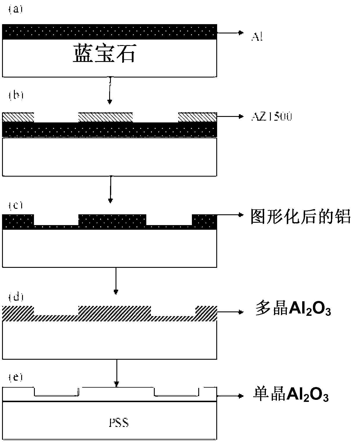
[0042] Prepare a patterned sapphire substrate for nitride epitaxial growth in the following order:
[0043] (1) Sputtering metal aluminum film: Use DC magnetron sputtering technology to magnetron sputter metal aluminum film of about 200nm on one surface of the sapphire substrate.
[0044] (2) Laser interference lithography: spin-coat AZ1500 photoresist on the sapphire substrate aluminum film sputtered with metal aluminum film in step (1), with a thickness of about 200nm, spin the glue at a speed of 2000r / min, and dry at 110°C for 2min; then Two laser interference exposures, the laser wavelength λ is 325nm, the exposure pattern is designed as a periodic circle, the exposure pattern period is 1μm, and the two laser beams are incident at a symmetrical angle with respect to the z axis ±θ is 9.35°, and the photoresist is processed. For the first exposure, the exposure time is 8 min, and then the substrate is rotated by 90°, and the photoresist is exposed for the second time with th...
Embodiment 2
[0049] Prepare a patterned sapphire substrate for nitride epitaxial growth in the following order:
[0050] (1) Sputtering metal aluminum film: Use DC magnetron sputtering technology to magnetron sputter metal aluminum film of about 200nm on one surface of the sapphire substrate.
[0051] (2) Laser interference lithography: spin-coat AZ1500 photoresist on the sapphire substrate aluminum film sputtered with metal aluminum film in step (1), with a thickness of about 200nm, spin the glue at a speed of 2000r / min, and dry at 110°C for 2min; then Two laser interference exposures, the laser wavelength λ is 325nm, the exposure pattern is designed as a periodic circle, the exposure pattern period is 1μm, and the two laser beams are incident at a symmetrical angle with respect to the z axis ±θ is 9.35°, and the photoresist is processed. For the first exposure, the exposure time is 8 min, and then the substrate is rotated by 90°, and the photoresist is exposed for the second time with th...
Embodiment 3
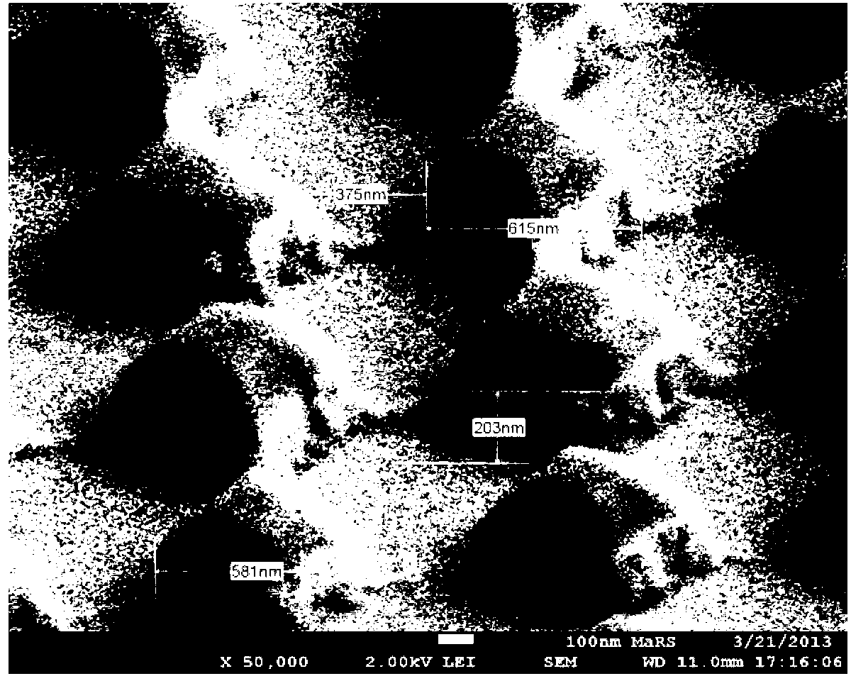
[0056] Crystal Structure Testing
[0057] The crystal structure of the prepared patterned sapphire substrate was tested by high-resolution X-ray diffractometer. Figure 6 is the scanning result of the patterned sapphire substrate (11-23) (11-23 is the crystal plane mark), Figure 7 It is the XRD-ω / 2θ scanning result of the patterned sapphire substrate (0006) (0006 is the crystal plane mark), and the result shows that the diffraction peak width at half maximum of the patterned sapphire substrate (0006) is FWHM=0.0101°. Figure 8 It is the XRD-ω / 2θ scanning result of the unpatterned sapphire substrate (0006), and the result shows that the half maximum width of the diffraction peak of the unpatterned sapphire substrate (0006) is FWHM=0.0133°. Figure 6 The XRD-Φ scanning results of the patterned sapphire substrate (11-23), the angle between (11-23) and (0006) crystal planes The sample is scanned from 0 to 360° around the surface normal n. exist Figure 6 There are 6 diffract...
PUM
| Property | Measurement | Unit |
|---|---|---|
| Thickness | aaaaa | aaaaa |
| Thickness | aaaaa | aaaaa |
Abstract
Description
Claims
Application Information