Manufacturing method of multi-wavelength laser array chip

A technology of multi-wavelength lasers and array chips, applied in the direction of laser devices, semiconductor laser devices, optical waveguide semiconductor structures, etc., can solve the problems of high device manufacturing costs, difficulty in mass production and application, and high cost of electron beam exposure technology. Achieve the effect of low-loss multi-wavelength emission

Active Publication Date: 2013-09-18
INST OF SEMICONDUCTORS - CHINESE ACAD OF SCI
View PDF4 Cites 30 Cited by
  • Summary
  • Abstract
  • Description
  • Claims
  • Application Information

AI Technical Summary

Problems solved by technology

However, the electron beam lithography technique has the disadvantage of high cost and low efficiency, and the disadvantage of the butt-coupled technique is that the growth conditions require exhaustive optimization.
The complex process leads to high device manufacturing costs, making it difficult to mass produce and apply

Method used


Image

  • Manufacturing method of multi-wavelength laser array chip
  • Manufacturing method of multi-wavelength laser array chip
  • Manufacturing method of multi-wavelength laser array chip

Examples


Embodiment 1

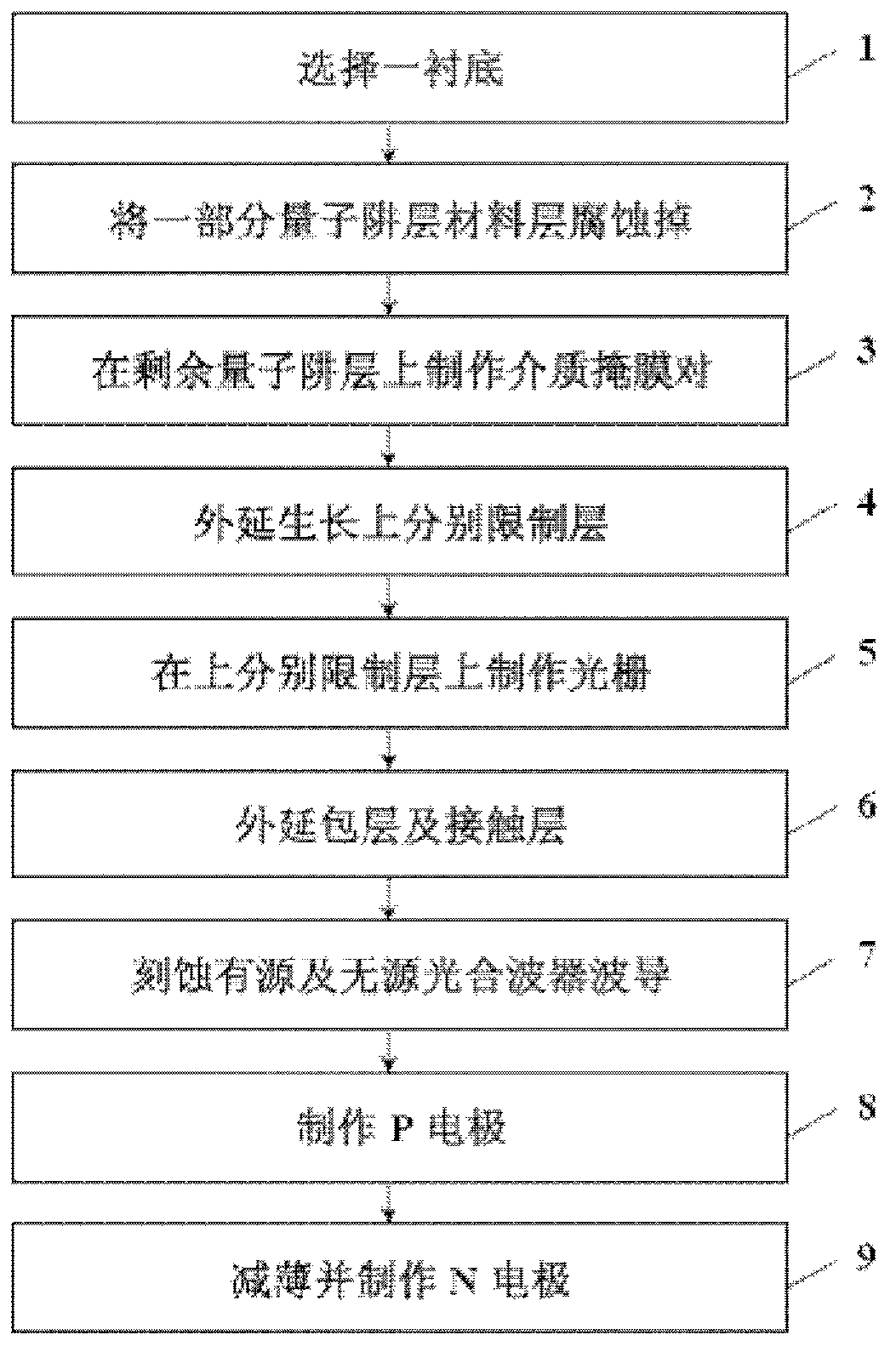
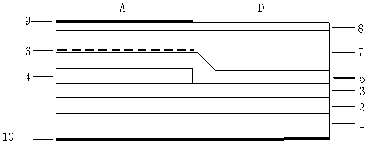
[0037] see figure 1 and Figure 3 to Figure 8 As shown, the present invention provides a method for manufacturing a multi-wavelength laser array chip, comprising the steps of:

[0038] Step 1: growing a buffer layer 2 , a lower confinement layer 3 and a multiple quantum well layer 4 on a substrate 1 . The material of the substrate 1 is GaAs, InP, GaN, SiC or Si.

[0039] Step 2: Etching a part of the multi-quantum well layer 4, the etched part is the passive optical combiner region D, and the remaining part is the active region A;

[0040] Step 3: making a dielectric mask pair Ma( Figure 7 ) or Mb( Figure 8 ). Dielectric mask pair patterns appear in pairs at the interval of array unit s, and for mask pattern Ma( Figure 7 ) in which the distance between the mask pairs remains constant, and the mask width increases gradually, that is, the widths of the masks M1, M2, M3 to MN satisfy W1 Figure 8 ) in which the mask width is constant and the distance between mask pairs is...

Embodiment 2

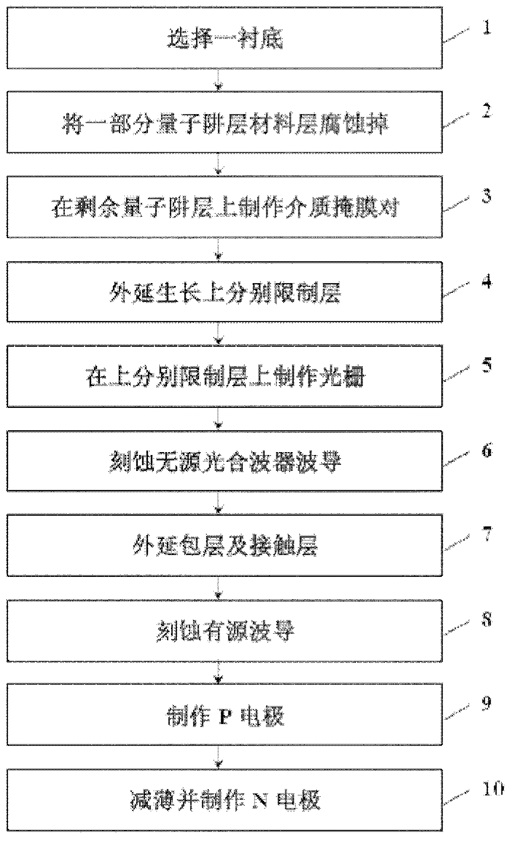
[0051] see again Figure 2 to Figure 8 As shown, the present invention provides a method for manufacturing a multi-wavelength laser array chip, comprising the steps of:

[0052] Step 1: growing a buffer layer 2 , a lower confinement layer 3 and a multiple quantum well layer 4 on a substrate 1 . The material of the substrate 1 is GaAs, InP, GaN, SiC or Si;

[0053] Step 2: Etching a part of the multi-quantum well layer 4, the etched part is the passive optical combiner region D, and the remaining part is the active region A;

[0054] Step 3: making a dielectric mask pair Ma( Figure 7 ) or Mb( Figure 8 ). Dielectric mask pair patterns appear in pairs at the interval of array unit s, and for mask pattern Ma( Figure 7 ) in which the distance between the mask pairs remains constant, and the mask width increases gradually, that is, the widths of the masks M1, M2, M3 to MN satisfy W1 Figure 8 ) in which the mask width is constant and the distance between mask pairs is gradual...


PUM


Abstract

A manufacturing method of a multi-wavelength laser array chip includes the steps of firstly, sequentially growing a buffer layer, a lower separate confinement layer and a multiple quantum well layer on a substrate; secondly, corroding part of the multiple quantum well layer, and using the corroded part as a passive optical combiner area and the rest part as an active area; thirdly, manufacturing medium mask pairs on the remained multiple quantum well layer; fourthly epitaxially growing an upper separate confinement layer on the upper surface of each of the passive optical combiner area and the active area; fifthly, removing the exposed medium mask pairs, and manufacturing gratings on the upper separate confinement layer on the active area; sixthly, extending a wrapping layer and a contact layer on each upper separate confinement layer; seventhly, etching an active waveguide on the contact layer of the active area, and etching a passive optical combiner waveguide on the contact layer of the passive optical combiner area; eighthly, manufacturing P electrodes on the active waveguide; ninthly, thinning the substrate, and manufacturing N electrodes at the back of the thinned substrate.

Description

technical field [0001] The invention relates to the field of optoelectronic devices, in particular to a method for manufacturing a multi-wavelength laser array chip. Background technique [0002] The multi-wavelength laser with monolithic integrated passive optical multiplexer is the core device of modern wavelength division multiplexing (WDM) optical communication system, which has the advantages of compact structure, low optical and electrical connection loss, high stability and reliability. This monolithic integrated device includes two parts: a laser array and a multiplexer. The light emitted by each laser is combined by the multiplexer and output by a single waveguide. The fabrication of the laser array requires that each laser has a different emission wavelength, and the fabrication of the multiplexer requires that the light can be transmitted in it with low loss. Therefore, the emission wavelength of the material of the multiplexer is generally much smaller than the e...

Claims


Application Information

Patent Timeline
Patent Type & Authority Applications(China)
IPC IPC(8): H01S5/40H01S5/20
Inventor 梁松张灿韩良顺朱洪亮王圩
Owner INST OF SEMICONDUCTORS - CHINESE ACAD OF SCI
Why Eureka
Try Eureka