Method for preparing diamond base FET device with T-similar-type grid shelter autocollimation technology

A diamond, self-aligned technology, used in semiconductor devices, semiconductor/solid-state device manufacturing, electrical components, etc., to solve problems such as increased resistance and decreased frequency performance of transistors

Active Publication Date: 2013-09-25
THE 13TH RES INST OF CHINA ELECTRONICS TECH GRP CORP
View PDF3 Cites 8 Cited by
  • Summary
  • Abstract
  • Description
  • Claims
  • Application Information

AI Technical Summary

Problems solved by technology

Realizing transistors on polycrystalline CVD self-supporting diamond materials, in order to achieve high-frequency performance, it is necessary to reduce the size of the device, while the size of the device is reduced, the gate-source and gate-drain resistance increases, and the frequency performance of the transistor decreases

Method used


Image

  • Method for preparing diamond base FET device with T-similar-type grid shelter autocollimation technology
  • Method for preparing diamond base FET device with T-similar-type grid shelter autocollimation technology
  • Method for preparing diamond base FET device with T-similar-type grid shelter autocollimation technology

Examples


Embodiment 1

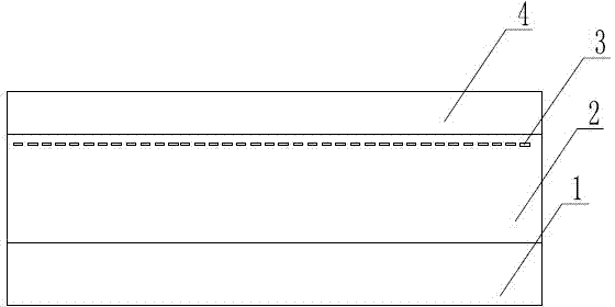
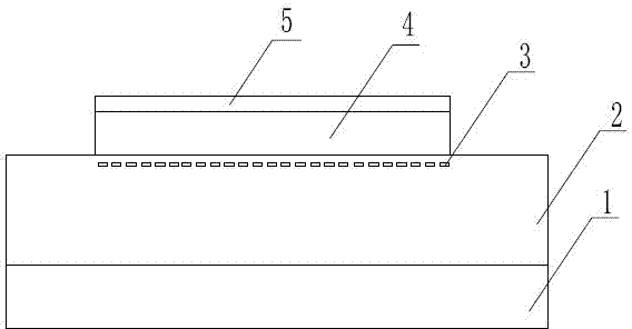
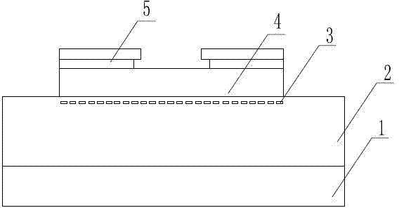
[0046] Example 1: (1) Using a microwave plasma chemical vapor deposition device to grow a high-resistance polycrystalline diamond of 300 μm on a molybdenum substrate; (2) Using hydrogen plasma for 30 minutes to form a p-type conductive channel on a high-resistance diamond material ; (3) Cover a layer of Au mask layer on the surface of the diamond material with a thickness of 2 μm; (4) Photolithography table; (5) Use KI+I 2 After the etching solution removes the Au mask in the area outside the mesa, use oxygen plasma etching equipment to etch for 2 minutes to achieve mesa isolation; (6) photolithographically etch the gate on the gold mask layer; (7) use KI to etch (8) Make a T-like gate in the above corrosion area, and the gate metal is Al; (9) The outer layer of the Al gate is oxidized in the air to form Al 2 o 3 (10) Using a T-shaped gate as a mask, using a self-alignment process, evaporating Au with a thickness of 5nm, self-aligning outside the shadow under the gate cap to ...

Embodiment 2

[0047] Example 2: (1) Using a microwave plasma chemical vapor deposition device to grow a high-resistance polycrystalline diamond of 300 μm on a molybdenum substrate; (2) Using hydrogen plasma for 30 minutes to form a p-type conductive channel on a high-resistance diamond material ; (3) Cover a layer of Ti mask layer on the surface of the diamond material, with a thickness of 2 μm; (4) Photolithographic mesa; (5) After removing the Ti mask in the area outside the mesa with hydrofluoric acid solution, use oxygen plasma etching equipment Etching is performed for 2 minutes to achieve mesa isolation; (6) Photoetching the gate on the Ti mask layer; (7) Using hydrofluoric acid solution to remove the Ti mask in the middle region of the source and drain; (8) In the above-mentioned etched area To make a T-like grid, the gate metal is Al; (9) the outer layer of the Al grid is oxidized in the air to form Al 2 o 3(10) Using a T-like gate as a mask, using a self-alignment process, evapora...


PUM

PropertyMeasurementUnit
thicknessaaaaaaaaaa

Abstract

The invention discloses a method for preparing a diamond base FET device with the T-similar-type grid shelter autocollimation technology, and relates to the technical field of methods for manufacturing semiconductor devices. The method comprises the step of forming a high-resisting diamond layer on a high temperature resistance substrate, the step of forming a conducting channel in the high-resisting diamond layer, the step of covering the surface of the high-resisting diamond layer with a metal mask layer, the step of photoetching a table-board, the step of removing a metal mask outside the table-board area through corrosive liquid, the step of forming grids on the metal mask in a photoetching mode, the step of removing the metal mask in the middle of a source leaking area through the corrosive liquid and forming source leakage, the step of manufacturing the T-similar-type grids in the corrosion area, the step of oxidizing or nitriding the outer sides of metal grids and forming a dielectric layer, and the step of enabling the T-similar-type grids to serve as a shield. According to the method, the T-similar-type grid shelter autocollimation technology is adopted, the distance between a grid source position and a grid leakage position is effectively shortened and is basically equal to the grid length, and the grid source resistance and grid leak resistance are reduced.

Description

technical field [0001] The invention relates to the technical field of manufacturing methods of semiconductor devices. Background technique [0002] Devices based on single crystal, polycrystalline and nanocrystalline diamond are collectively referred to as diamond-based devices, such as diamond MESFET, MISFET, JFET, etc. Diamond-based devices have the advantages of high operating temperature, strong breakdown field, high cut-off frequency, and high power density, and are the first choice for the future microwave high-power field. To realize transistors on polycrystalline CVD self-supporting diamond materials, to achieve high-frequency performance, it is necessary to reduce the size of the device, while the size of the device is reduced, the gate-source and gate-drain resistances increase, and the frequency performance of the transistor decreases. Contents of the invention [0003] The technical problem to be solved by the present invention is to provide a method for prep...

Claims


Application Information

Patent Timeline
Patent Type & Authority Applications(China)
IPC IPC(8): H01L21/336H01L21/28
Inventor 冯志红王晶晶何泽召李佳
Owner THE 13TH RES INST OF CHINA ELECTRONICS TECH GRP CORP
Why Eureka
Try Eureka