High-power semiconductor laser transition heat sink and preparation method thereof

A laser and semiconductor technology, applied in semiconductor lasers, structural details of semiconductor lasers, lasers, etc., can solve problems such as metal connection, laser damage, bar damage, etc., to achieve accurate size, smooth upper and lower surfaces, and accuracy better than Effect

Active Publication Date: 2013-09-25
Shandong Huaguang Optoelectronics Co. Ltd.
View PDF8 Cites 5 Cited by
  • Summary
  • Abstract
  • Description
  • Claims
  • Application Information

AI Technical Summary

Problems solved by technology

[0005] The Chinese patent document CN102074890A "A Method for Packaging Die Series Lasers" proposes a method of using SiC as a transitional heat sink. This invention solves the problem that the transitional heat sink cannot be guaranteed by directly evaporating a titanium gold layer on the top and bottom surfaces of the transitional heat sink. The insulation of the side is easy to cause the problem of metal connection between the upper and lower sides. A new method is proposed to directly carry out metallization on the whole SiC crystal, and then make the required insulating groove by photolithography or ion etching. Finally The required transitional heat sink is obtained by dividing the SiC crystal, which ensures the insulation of the upper and lower sides
However, this method uses physical destruction to insulate the bar, which is easy to cause damage to the bar, and the hardness of SiC is very large, close to that of diamond. It is very difficult to cut directly by physical methods, which is easy to cause damage to the laser and must be determined according to the conditions of the bar. Cut size is very limited

Method used


Image

  • High-power semiconductor laser transition heat sink and preparation method thereof
  • High-power semiconductor laser transition heat sink and preparation method thereof
  • High-power semiconductor laser transition heat sink and preparation method thereof

Examples


Embodiment 1

[0042] Embodiment 1. A method for manufacturing a high-power laser single-die transitional heat sink.

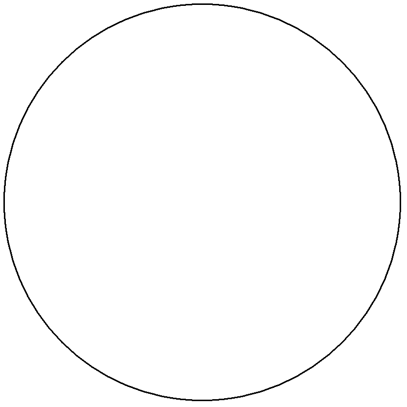
[0043] (1) Cut the SiC crystal with a single-wire swing cutting machine to obtain a SiC wafer with a flat upper and lower surface, a thickness of 400 μm, and a diameter of 2.5 inches. like figure 1 shown.

[0044] (2) Clean the SiC wafer obtained in step (1), soak the SiC wafer in sulfuric acid with a concentration of 90 wt% for half an hour, rinse the sulfuric acid on the surface with deionized water and blow dry with nitrogen.

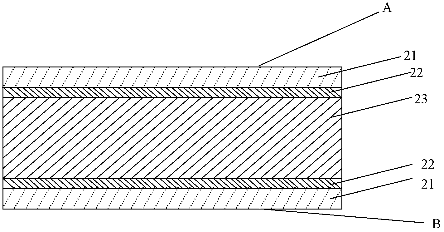
[0045] (3) The cleaned SiC wafer 23 is vapor-deposited metal titanium on the upper and lower surfaces respectively as a metal transition layer 22 with a thickness of 50 μm by vapor deposition; is 300μm; the metallized SiC wafer is obtained, and the cross-sectional view is as follows figure 2 As shown, the upper and lower surfaces of the wafer are A-side and B-side respectively.

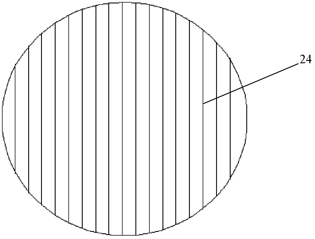
[0046] (4) Making insulating grooves 24 on the surface A of the ...

Embodiment 2

[0049] Embodiment 2. A method for preparing a high-power laser dual-die transitional heat sink.

[0050] As described in Embodiment 1, step (5) divides the finished product monolithic wafer obtained in step (4) into a single transitional heat sink for double-die encapsulation, Figure 5 Shown is a dual die transition heat sink that was laser scribed to image 3 The overall wafer shown is scribed and divided into Figure 5 The shape shown is cut with a straight line perpendicular to the insulation groove, a straight line parallel to the insulation groove, and a straight line where the insulation groove is located. Two insulation slots are reserved between the wires, which are used to wire the soldered die to the left side of the insulation slot, which is convenient for die stick testing and improves the subsequent packaging pass rate.

Embodiment 3

[0051] Embodiment 3, a preparation method of a high-power laser multi-die transitional heat sink

[0052] Steps (1), (2) are as in Example 1. The difference is:

[0053] (3) The cleaned SiC wafer 23 is vapor-deposited metal titanium on the upper and lower surfaces respectively as a metal transition layer 22 by vapor deposition, with a thickness of 45 μm; It is 200μm; the metallized SiC wafer is obtained, and the cross-sectional view is as follows figure 2 As shown, the upper and lower surfaces of the wafer are A-side and B-side respectively.

[0054] (4) Making insulating grooves 24 on the surface A of the metallized SiC wafer obtained in step (3) by ion etching, the width of the insulating grooves is 0.8 mm, and the interval of the insulating grooves is 3 mm. like image 3 shown. The depth of the insulating trench exposes the SiC wafer.

[0055] The method of ion etching is to use plasma to etch thin films. The plasma is accelerated by an electric field so that it has ...


PUM

PropertyMeasurementUnit
thicknessaaaaaaaaaa
diameteraaaaaaaaaa
thicknessaaaaaaaaaa

Abstract

The invention provides a high-power semiconductor laser transition heat sink and a preparation method thereof. The transition heat sink comprises a substrate, a metal transition layer and a welding flux adhering layer. The substrate consists of an SiC wafer, a titanium metal transition layer or a chromium metal transition layer and a gold welding flux adhering layer are sequentially arranged on the upper surface and the lower surface of the SiC wafer respectively in an evaporation mode, the upper surface and the lower surface of the SiC wafer are an A face and a B face respectively, and an insulated slot is manufactured in the A face. The preparation method includes the steps of conducting wire-electrode cutting on the SiC wafer to cut the SiC wafer into a wafer, washing the wafer, conducting surface metallization on the SiC wafer, etching the insulated slot in the A face of the metallized wafer, and forming the single laser transition heat sink in a dividing mode. The heat-conducting property of the high-power semiconductor laser transition heat sink based on the SiC wafer is better than the heat-conducting property of a transition heat sink of an aluminum nitride ceramic substrate, the size is accurate, and the size can be determined flexibly according to the packaging need of a high-power laser.

Description

technical field [0001] The invention relates to a transitional heat sink for packaging a high-power semiconductor laser and a preparation method thereof, belonging to the technical field of semiconductor lasers. Background technique [0002] With the advent of lasers, laser technology has been widely used in various technical fields. Due to the advantages of small size, high power, and stable performance, semiconductor lasers have been widely used in various fields such as industry, medicine, and military affairs. With the continuous maturity of laser packaging technology, the required laser power continues to increase, and the difficulty of laser packaging is also getting higher and higher. To meet the demand for high power lasers, there are generally two solutions, connecting semiconductor chips in parallel or in series. The method of parallel connection is to use the metal heat sink as the substrate to weld the semiconductor chip on it to achieve the purpose of parallel ...

Claims


Application Information

Patent Timeline
Patent Type & Authority Applications(China)
IPC IPC(8): H01S5/024H01S5/02
Inventor 王娜李沛旭夏伟汤庆敏
Owner Shandong Huaguang Optoelectronics Co. Ltd.
Why Eureka
Try Eureka