
Method for preparing CIGS (copper indium gallium selenide) film through selenylation at low temperature

A technology of selenization and thin film, applied in the direction of final product manufacturing, sustainable manufacturing/processing, ion implantation plating, etc., can solve the problems of difficult removal of surfactants, high toxicity, flammability and explosion, etc., and achieve selenization effect Good, eliminate grain boundaries, low toxicity and safe selenization temperature effect

Active Publication Date: 2013-10-02
徐东
View PDF4 Cites 18 Cited by
  • Summary
  • Abstract
  • Description
  • Claims
  • Application Information

AI Technical Summary

Problems solved by technology

[0011] In the prior art, the particle method is to use different particle sizes of copper, indium, gallium, selenium or their binary, ternary or quaternary alloy nanoparticles to make printing ink, and then prepare the copper indium gallium selenium absorbing layer of thin film solar cells , to obtain a thin film by rapid heat treatment. The problem with this method is that the residual surfactant is not easy to remove when preparing CIGS nanocrystalline particles in the traditional selenization atmosphere, and it is easy to cause carbon residues between the grain boundaries, which makes it difficult to form larger particles. CIGS particles and formation of continuous CIGS films
Se vapor is less toxic, but less effective; while H 2 Although Se selenization effect is good, but H 2 Se is highly toxic, flammable and explosive

Method used


Image

  • Method for preparing CIGS (copper indium gallium selenide) film through selenylation at low temperature
  • Method for preparing CIGS (copper indium gallium selenide) film through selenylation at low temperature
  • Method for preparing CIGS (copper indium gallium selenide) film through selenylation at low temperature

Examples


preparation example Construction

[0052] 1. In the preparation method of the present invention, the ratio of copper, indium, gallium, and selenium elements can be adjusted to obtain CIGS nanocrystals with adjustable band gap, and the multi-layer film can be coated on the substrate, so that the finally prepared CIGS thin film can become a gradient distribution. Composite CIGS thin film, thereby greatly improving the efficiency of CIGS thin film solar cells;

[0053] 2. In the prior art, the selenization of the solid selenium source requires a higher temperature to evaporate the selenium source into steam for selenization. However, the low-temperature selenization of the present invention is carried out at a low temperature of 100-400°C, which is convenient for low tolerance The film is coated on the flexible substrate, and the alcohol solvent will dissolve the residual alkylamine in the CIGS precursor film during the heating process, so as to solve the problem of carbon residue in the CIGS film prepared by the n...

Embodiment 1

[0057] A method for preparing CIGS film by low-temperature selenization, comprising the steps of:

[0058] (1) Preparation of CIGS nanocrystals:

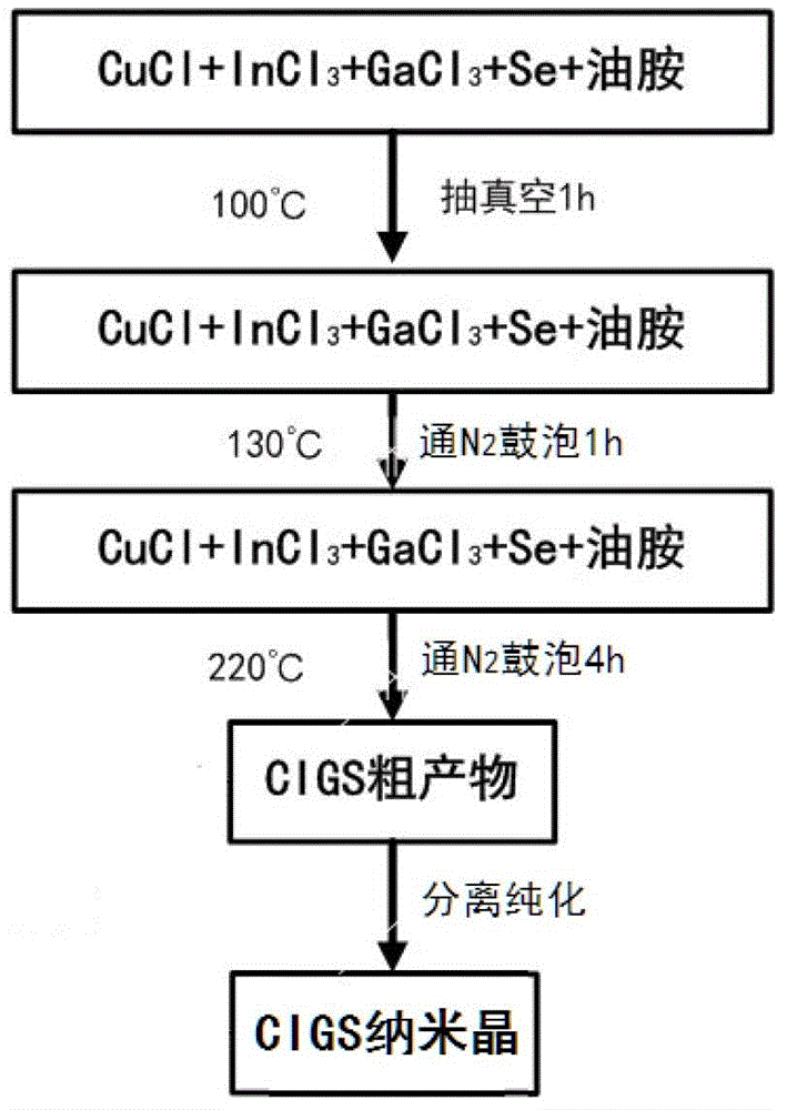
[0059] The preparation process of CIGS nanocrystals is as follows: figure 1 shown in the rich N 2 In the glove box, weigh 10mmol CuCl, 7mmol InCl 3 , 3mmol GaCl 3 and 20mmol Se, mixed and placed in a 250mL three-neck flask with a condenser tube and a stopcock, the flask was removed after closing the stopcock, the stopcock port was immediately connected to the Schlenk tube, and then the flask was wrapped with quartz wool and placed in a heating mantle. Inject another 100ml of oleylamine, open the piston and heat to 100°C, vacuumize at -0.1MPa vacuum for 1h, and then2 Heat to 130°C with magnetic stirring for 1 hour under bubbling, remove water and oxygen, heat up to 220°C and stir vigorously for 4 hours, remove the heating mantle, cool to room temperature to obtain a suspension, separate and purify to obtain CIGS nanocrystals;

[...

Embodiment 2

[0068] A method for preparing CIGS film by low-temperature selenization, comprising the steps of:

[0069] (1) Preparation of CIGS nanocrystals:

[0070] Reference for the preparation process of CIGS nanocrystals figure 1 , in rich N 2 In a glove box, weigh 2mmol copper acetylacetonate, 0.18mmol indium acetylacetonate, 0.2mmol gallium acetylacetonate and 4mmolSe, mix them and place them in a 100mL three-necked flask with a condenser tube and a stopcock, remove the flask after closing the stopcock, and immediately remove the stopcock Connect the mouth of the flask to the Schlenk tube, then wrap the flask with quartz wool and place it in a heating mantle, inject 10ml of octadecylamine, open the piston and heat to 60°C, vacuumize at -0.1MPa for 3h, and then N 2 Heat to 100°C with magnetic stirring for 3 hours under bubbling, remove water and oxygen, heat up to 300°C and vigorously stir for 1 hour, remove the heating mantle, cool to room temperature to obtain a suspension, sepa...


PUM

PropertyMeasurementUnit
Thicknessaaaaaaaaaa
Thicknessaaaaaaaaaa
Thicknessaaaaaaaaaa

Abstract

The invention discloses a method for preparing a CIGS (copper indium gallium selenide) film through selenylation at low temperature. The method comprises the following steps of carrying out a reaction on a copper resource, an indium resource, a gallium resource and a selenium resource as well as alkylamine so as to obtain CIGS nanocrystalline, mixing the CIGS nanocrystalline with a solvent so as to obtain CIGS nanocrystalline ink, coating so as to obtain a coating substrate, then carrying out steam inducing low temperature selenylation: putting the coating substrate and an organic selenium alcoholic solution independently in a closed environment, heating to 100-400 DEG C, carrying out a selenylation reaction through full contact of the steam generated by the organic selenium alcoholic solution and the coating substrate, and obtaining the CIGS film. By adopting steam inducing selenylation, the method has the advantages of good selenylation effect, low toxicity and safety as well as lower selenylation temperature, and is convenient to coat the film on a low temperature enduring flexible substrate. The photoelectric conversion efficiency can be improved when obtained CIGS films are used for preparing solar energy batteries.

Description

technical field [0001] The invention relates to the field of new energy sources of optoelectronic materials, in particular to a method for preparing CIGS thin films by low-temperature selenization. Background technique [0002] At present, due to the impact of the global energy crisis, solar energy has become a hot spot for alternative energy. Copper indium sulfide (CIS) thin-film solar cells (including copper indium sulfide, copper gallium selenide, copper gallium sulfide, copper indium gallium selenide (hereinafter referred to as CIGS), copper indium gallium sulfide and copper indium gallium sulfide selenide, etc.) The optoelectronic properties and structural stability of the material are recognized as one of the most promising third-generation photovoltaic materials. At present, the highest efficiency of CIGS thin-film solar cells is 20.3% created by the traditional vacuum process, but because the traditional vacuum process cannot overcome high cost, high equipment requi...

Claims


Application Information

Patent Timeline
IPC IPC(8): C23C14/06H01L31/18H01L31/032
CPCY02P70/50
Inventor 徐东徐永清陈雄
Owner 徐东
Learn More