Ultrathin VSOP (very thin small outline package) packaging part and production method thereof
A production method and ultra-thin technology, applied in the direction of electrical components, semiconductor devices, electric solid devices, etc., can solve the problems of low packaging yield and high cost of small lead-out wire packaging, and achieve the effect of preventing product deviation and avoiding suspension
- Summary
- Abstract
- Description
- Claims
- Application Information
AI Technical Summary
Problems solved by technology
Method used
Image

Examples
Embodiment 1
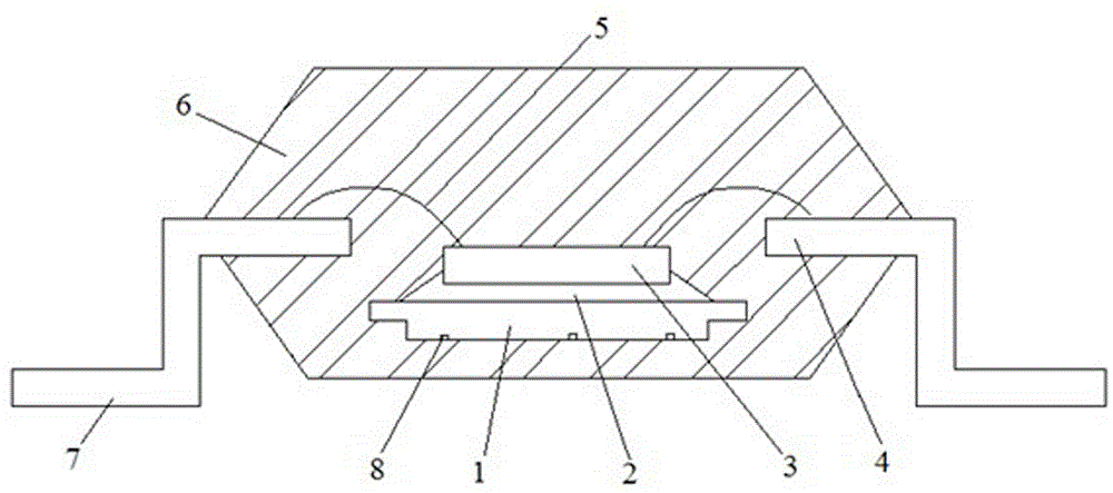
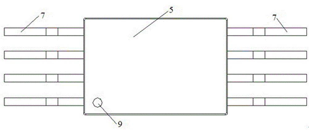
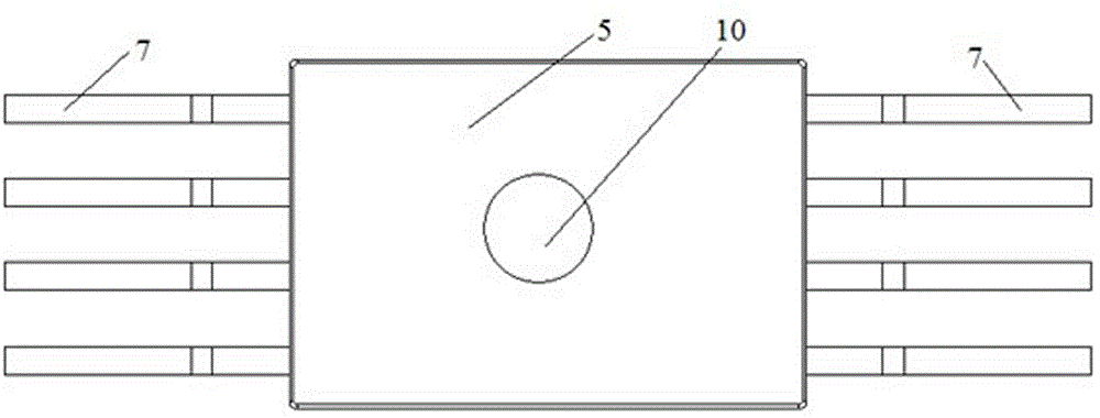
[0067] Through rough grinding, fine grinding and polishing, a wafer with a final thickness of 150 μm is obtained; during rough grinding, the rough grinding speed is 100 μm / min, and the rough grinding thickness ranges from the original wafer thickness + film thickness to 200 μm + film thickness; When grinding, the accuracy speed is 9μm / min, and the precision thickness ranges from 200μm + film thickness to 160μm + film thickness; when polishing, mechanical polishing is performed first, and then chemical polishing; polishing thickness ranges from 160μm + film thickness to 150μm + film thickness Thickness, the process of preventing chip warpage is adopted in the process of wafer thinning. Use DISC 3350 dicing machine to dicing the thinned wafers, set anti-fragmentation and anti-crack scribing optimization parameters through DOE optimization, scribing feed speed 6mm / s, clean and dry in time after scribing; take Stamped multi-row copper alloy electroplating lead frame with anti-spla...
Embodiment 2
[0079] Through rough grinding, fine grinding and polishing, a wafer with a final thickness of 170 μm is obtained; during rough grinding, the rough grinding speed is 75 μm / min, and the rough grinding thickness ranges from the original wafer thickness + film thickness to 220 μm + film thickness; When grinding, the accuracy speed is 10μm / min, and the precision thickness ranges from 220μm + film thickness to 180μm + film thickness; when polishing, mechanical polishing is performed first, and then chemical polishing; polishing thickness ranges from 180μm + film thickness to 170μm + film thickness Thickness, the process of preventing chip warpage is adopted in the process of wafer thinning. Use DISC 3350 dicing machine to dicing the thinned wafers, set anti-fragmentation and anti-crack scribing optimization parameters through DOE optimization, scribing feed speed 10mm / s, clean and dry in time after scribing; take Stamped multi-row nickel-palladium-gold electroplated lead frame with ...
Embodiment 3
[0081] Through rough grinding, fine grinding and polishing, a wafer with a final thickness of 160 μm is obtained; during rough grinding, the rough grinding speed is 50 μm / min, and the rough grinding thickness ranges from the original wafer thickness + film thickness to 210 μm + film thickness; When grinding, the accuracy speed is 8μm / min, and the accuracy thickness ranges from 210μm + film thickness to 170μm + film thickness; when polishing, mechanical polishing is performed first, and then chemical polishing; polishing thickness ranges from 170μm + film thickness to 160μm + film thickness Thickness, the process of preventing chip warpage is adopted in the process of wafer thinning. Use DISC 3350 dicing machine to dicing the thinned wafers, set anti-fragmentation and anti-crack scribing optimization parameters through DOE optimization, scribing feed speed 8mm / s, clean and dry in time after scribing; take Stamped multi-row silver-plated lead frame with anti-spill film attached ...
PUM
 Abstract
Description
Claims
Application Information