
A photovoltaic thin film backplane

A photovoltaic film and backplane technology, applied in photovoltaic power generation, electrical components, circuits, etc., can solve the problems of low photoelectric conversion efficiency, thick thickness, large weight, etc., to improve photoelectric conversion efficiency, reduce wall thickness uniformity, reduce The effect of weight

Inactive Publication Date: 2015-10-28
中国科学院宁波材料技术与工程研究所湖州新能源产业创新中心
View PDF6 Cites 0 Cited by
  • Summary
  • Abstract
  • Description
  • Claims
  • Application Information

AI Technical Summary

Problems solved by technology

[0003] However, the battery components using TPT film and TPE film as the back plate have the defect of low photoelectric conversion efficiency, while the battery components using glass and aluminum materials as the back plate are thick and heavy
[0004] In order to further increase the utilization rate of sunlight per unit area, and improve the overall photoelectric conversion efficiency of battery components, especially crystalline silicon battery components, the invention patent application with the application publication number of CN102306671A discloses an integrated solar backplane. The aluminum backplane is provided with a reflective layer on the surface of the aluminum backplane, which is used to reflect the sunlight passing through the solar thin film battery chip in the module back to the solar thin film battery chip in the form of diffuse reflection; A solar photovoltaic module disclosed in the utility model patent of CN202721167U also proposes the idea of ​​setting a diffuse reflection part on the photovoltaic backplane; however, the above two solutions have no specific solutions for the reflective layer or the diffuse reflection part

Method used


Image

  • A photovoltaic thin film backplane
  • A photovoltaic thin film backplane
  • A photovoltaic thin film backplane

Examples


Embodiment 1

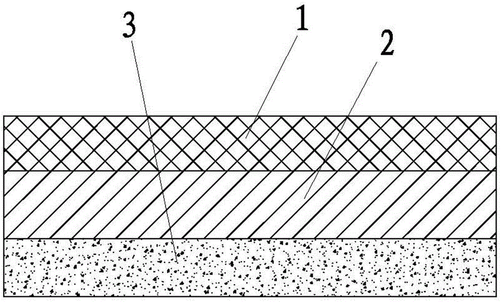
[0031] Embodiment 1: as figure 1 As shown, a photovoltaic thin film backboard includes a multi-microbubble polymer film layer 1, a PET film layer 2, and a fluorine-containing film layer 3 from top to bottom; The surface of the backsheet away from the cells is down.

[0032] Such as Figure 5 As shown in the figure, the abscissa is the wavelength, and the ordinate is the reflectivity. The a curve represents the diffuse reflection of sunlight on the surface of the tiny bubbles; the b curve represents the non-vertical reflection of sunlight on the surface of the tiny bubbles; the c curve Represents the vertical reflection of sunlight on the surface of tiny bubbles; it can be seen from the figure that the diffuse reflectance occurs between 95% and 97% in the wavelength range of 390-770 nanometers. It can be seen from the data that this embodiment has high diffuse reflectance performance.

[0033] Such as Figure 4 As shown, the top view of the surface topography of the multi-m...

Embodiment 2

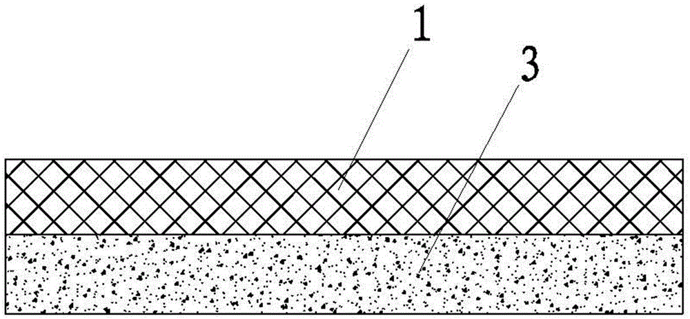
[0041] Embodiment 2: as figure 2As shown in the figure, a photovoltaic thin film backboard includes a multi-microbubble polymer film layer 1 and a fluorine-containing thin film layer 3 from top to bottom; when installed, the backplane surface close to the cell unit is on the top, and the backplane away from the cell unit is The plate surface is down.

[0042] Because the multi-microbubble polymer film layer 1 has a certain supporting effect, which realizes the supporting function of the current PET film in the back sheet, it can replace the PET film commonly used in the existing photovoltaic back sheet matrix materials, thereby realizing the photovoltaic thin film back sheet The two-layer structure not only saves costs and reduces consumables, but also makes the photovoltaic film backplane lighter and thinner, further reducing the consumables and weight ratio of the photovoltaic backplane.

[0043] The thickness of this embodiment is 1.2mm.

[0044] The preparation steps of...

Embodiment 3

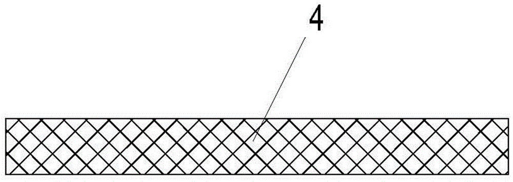
[0049] Embodiment 3: as image 3 As shown, a photovoltaic thin film backsheet is composed of a fluorine-containing multi-microbubble polymer film layer 4, which is made by foaming a fluorine-containing polymer, and has good anti-ultraviolet, waterproof, insulation, weather resistance and aging resistance, etc. performance, and also has a certain supporting effect, which can replace PET film, fluorine-containing film and other backsheet materials in the prior art at the same time, and realize a one-layer structure of photovoltaic thin film backsheet; this not only saves costs, but also makes the photovoltaic thin film backsheet more efficient. Light and thin, effectively reducing the consumables and weight ratio of photovoltaic backplanes.

[0050] The thickness of this embodiment is 0.3mm.

[0051] The preparation steps of the fluorine-containing multi-microbubble polymer film layer 1 of the present embodiment are as follows in sequence:

[0052] (1) Place the fluorine-conta...


PUM

PropertyMeasurementUnit
thicknessaaaaaaaaaa
thicknessaaaaaaaaaa
thicknessaaaaaaaaaa

Abstract

The invention relates to a component, particularly to a photovoltaic thin film backboard. The technical purpose of the invention is realized through the following technical scheme: the photovoltaic thin film backboard comprises a multi-microvesicle polymer film layer. The photovoltaic thin film backboard has high diffuse reflection performance to increase the use ratio of sunlight in unit area, to improve the integral photovoltaic conversion efficiency of a battery pack, particularly a crystal silicon battery pack; in addition, the photovoltaic thin film backboard is lower in cost and light in weight, and can effectively reduce the consumable items and weight ratio of photovoltaic backboards.

Description

technical field [0001] The invention relates to a photovoltaic module, in particular to a photovoltaic film backboard. Background technique [0002] Among solar cells, crystalline silicon solar cells account for about 90% of the solar cell market due to their high conversion rate and mature technology; traditional photovoltaic modules are generally layered structures, using glass, cells, EVA glue and backsheet materials It is made by lamination; the backplane material usually adopts TPT (structure is PVF / PET / PVF) composite film, TPE (structure is PVF / PET / EVA) composite film or glass, aluminum materials, etc.; for example, the application publication number is CN102938426A A solar photovoltaic backsheet material and its preparation method disclosed in the invention patent application of 2010, adopts the method of thermal compounding, firstly, fluoroplastics, EVA or PE plastics, and composite layer materials are plasticized, melted and extruded in an extruder , to obtain an i...

Claims


Application Information

Patent Timeline
Patent Type & Authority Patents(China)
IPC IPC(8): H01L31/048B32B27/08B32B9/04
CPCY02E10/50
Inventor 许炜郑文革张贤鹏吴秋萍宋伟杰王振卫刘涛
Owner 中国科学院宁波材料技术与工程研究所湖州新能源产业创新中心
Learn More