

Top grid self-alignment thin-film transistor with source/drain areas raised and manufacturing method thereof
A technology of thin film transistor and manufacturing method, which is applied in transistors, semiconductor/solid-state device manufacturing, semiconductor devices and other directions, can solve the problems of increasing off-state current of devices, increasing energy consumption, affecting channel devices, etc., and reducing off-state current. effect, avoid the increase of energy consumption, improve the effect of off-state characteristics
- Summary
- Abstract
- Description
- Claims
- Application Information
AI Technical Summary
Problems solved by technology
Method used
Image

Examples
Embodiment 1
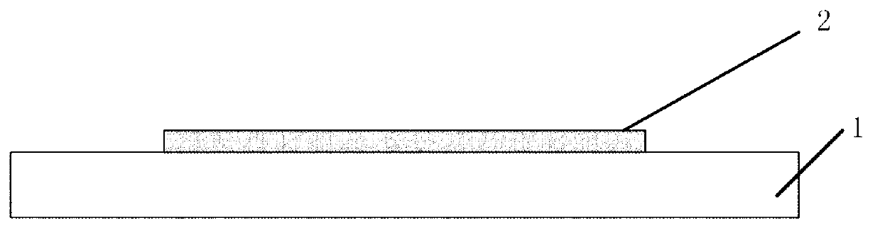
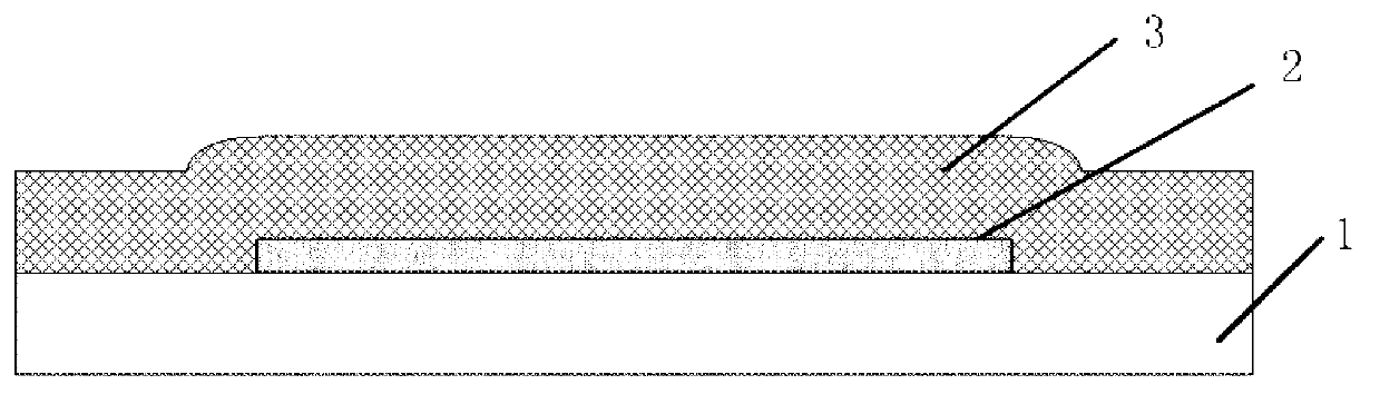
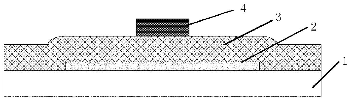
[0043] The cross-sectional view of the thin film transistor produced in this embodiment is as follows Figure 11 As shown, the thin film transistor is fabricated on a glass substrate 1 and includes an active layer 2 , a gate dielectric layer 3 , a gate electrode 4 , raised source regions 7 and drain regions 8 . Among them, the active layer region corresponding to the gate is the channel region, and the left and right sides of the channel region are respectively the source region and the drain region. the left and right sides of the layer. The active layer 2 is located on the glass substrate 1, and the active layer includes the channel region corresponding to the gate electrode and the source and drain regions on both sides of the channel region; the gate dielectric layer 3 is located on the active layer 2; the gate electrode 4 is located on the gate dielectric layer 3; the raised source region 7 and the raised drain region 8 are respectively located on the source region and t...
Embodiment 2
[0057] The cross-sectional view of the thin film transistor produced in this embodiment is as follows Figure 11 As shown, it is the same as in Embodiment 1, as described above.
[0058] The specific examples of the manufacturing process of the thin film transistor in this embodiment are as follows: figure 1 — Figure 4 with Figure 8 — Figure 13 shown. figure 1 — Figure 4 and Figure 12 — Figure 13 The manufacturing method has been described in detail in Example 1. In this example Figure 8 — Figure 11 The manufacturing process shown is different from that in Example 1, and will be described in detail below:
[0059] Such as Figure 8 As shown, a layer of positive photoresist is coated on the surface, and the opaque gate is used as a mask to expose from the back of the glass substrate ( Figure 8 The direction indicated by the middle arrow is the incident direction of the exposure light), and the photoresist 6 on the top of the grid remains after development. ...
PUM
| Property | Measurement | Unit |
|---|---|---|
| Thickness | aaaaa | aaaaa |
Abstract
Description
Claims
Application Information