Preparation method for InN/GaN/glass structure

A technology for glass and glass substrates, applied in the field of deposition and preparation of new optoelectronic materials, can solve the problems of high price of sapphire substrates, hinder the development of InN material devices, and difficult to reduce device costs, achieve good electrical performance and stability, and solve the problems of crystal Grid mismatch, low cost effect

Active Publication Date: 2013-10-16
辽宁太阳能研究应用有限公司
View PDF1 Cites 0 Cited by
  • Summary
  • Abstract
  • Description
  • Claims
  • Application Information

AI Technical Summary

Problems solved by technology

As we all know, the price of sapphire substrate is relatively high. Using it as the substrate of InN material makes it difficult to reduce the cost of InN material-based devices, which seriously hinders the development of InN material devices.

Method used


Image

  • Preparation method for InN/GaN/glass structure
  • Preparation method for InN/GaN/glass structure
  • Preparation method for InN/GaN/glass structure

Examples


Embodiment 1

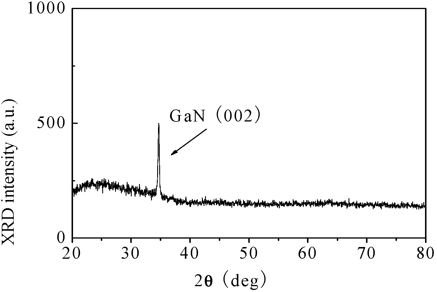
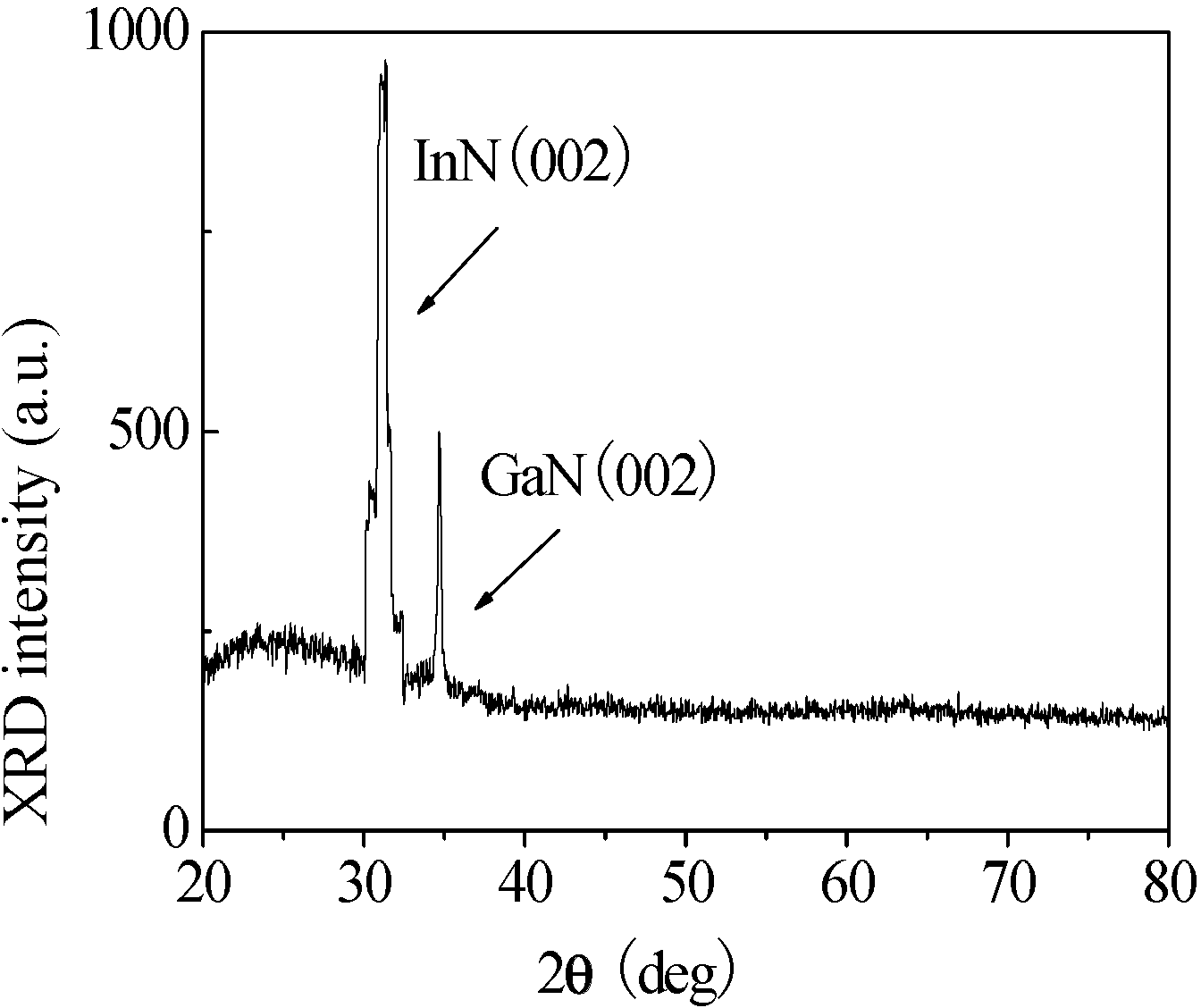
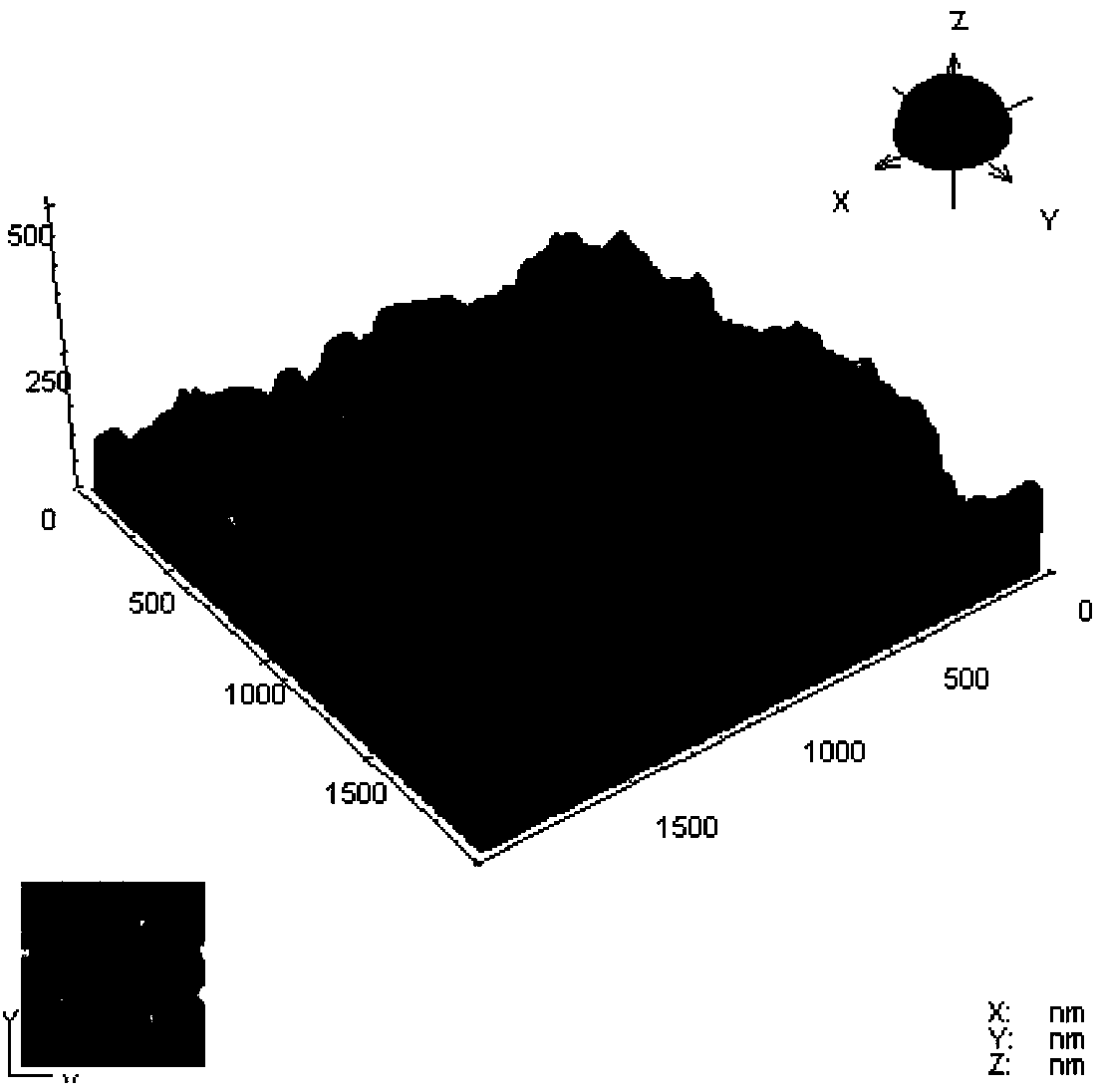
[0051] The Corning glass substrate was ultrasonically cleaned with acetone, ethanol and deionized water for 5 minutes, then dried with nitrogen and sent to the reaction chamber; the reaction chamber was evacuated to 9.0×10 -4 Pa, the substrate is heated to 485°C, trimethylgallium and nitrogen carried by hydrogen are introduced into the reaction chamber, and the flow rates of the two are 0.5sccm and 80sccm, controlled by a mass flow meter; the total pressure of the control gas is 1.2Pa; The electron cyclotron resonance power is 650W, and the reaction is 30min, and the GaN buffer layer film on the Corning glass substrate is obtained. Then continue to use the ECR-PEMOCVD system to evacuate the reaction chamber to 8.0×10 -4 Pa, the substrate is heated to 300°C, trimethylindium and nitrogen carried by hydrogen are introduced into the reaction chamber, the flow ratio of the two is 4:150, and the flow is 4sccm and 150sccm, controlled by a mass flow meter; control gas The...

Embodiment 2

[0054] The Corning glass substrate was ultrasonically cleaned with acetone, ethanol and deionized water for 5 minutes, then dried with nitrogen and sent to the reaction chamber; the reaction chamber was evacuated to 9.0×10 -4 Pa, the substrate is heated to 485°C, trimethylgallium and nitrogen carried by hydrogen are introduced into the reaction chamber, and the flow rates of the two are 0.6sccm and 90sccm, controlled by a mass flow meter; the total pressure of the control gas is 1.2Pa; The electron cyclotron resonance power is 650W, and the reaction is 30min, and the GaN buffer layer film on the Corning glass substrate is obtained. Then continue to use the ECR-PEMOCVD system to evacuate the reaction chamber to 8.0×10 -4 Pa, the substrate is heated to 200°C, trimethylindium and nitrogen carried by hydrogen are introduced into the reaction chamber, the flow ratio of the two is 4:120, and the flow rate is 4sccm and 120sccm, controlled by a mass flow meter; control gas...

Embodiment 3

[0056] The Corning glass substrate was ultrasonically cleaned with acetone, ethanol and deionized water for 5 minutes, then dried with nitrogen and sent to the reaction chamber; the reaction chamber was evacuated to 9.0×10 -4 Pa, the substrate is heated to 485°C, trimethylgallium and nitrogen carried by hydrogen are introduced into the reaction chamber, and the flow rates of the two are 0.5sccm and 120sccm, controlled by a mass flow meter; the total pressure of the control gas is 1.2Pa; The electron cyclotron resonance power is 650W, and the reaction is 30min, and the GaN buffer layer film on the Corning glass substrate is obtained. Then continue to use the ECR-PEMOCVD system to evacuate the reaction chamber to 8.0×10 -4 Pa, the substrate is heated to 100°C, trimethylindium and nitrogen carried by hydrogen are introduced into the reaction chamber, the flow ratio of the two is 5:120, and the flow is 5 sccm and 120 sccm, controlled by a mass flow meter; control gas ...


PUM

PropertyMeasurementUnit
thicknessaaaaaaaaaa

Abstract

The invention belongs to the technical field of novel photoelectric material sediment preparation, and provides a preparation method for an InN / GaN / glass structure which has excellent electric performance and stability. The preparation method comprises the following steps: 1), a glass substrate is subjected to ultrasonic cleaning by acetone, ethanol, and deionized water sequentially, and then is blow-dried by nitrogen gas and sent to a reaction chamber; 2), the reaction chamber is vacuumized by adopting an ECR-PEMOCVD system, the glass substrate is heated, and trimethyl gallium carried by hydrogen and nitrogen gas are introduced into the reaction chamber, wherein the flux of the trimethyl gallium and the flux of the nitrogen gas are 0.5 sccm-0.8 sccm and 80 sccm-120 sccm respectively, and the total pressure of the gas is controlled, a GaN buffer layer film of the glass substrate can be obtained after the reaction under the electron cyclotron resonance condition; 3), the reaction chamber is vacuumized by adopting the ECR-PEMOCVD system for the second time, the glass substrate is heated to 200-400 DEG C, and the trimethyl gallium carried by hydrogen and the nitrogen gas are pumped into the reaction chamber.

Description

technical field [0001] The invention belongs to the technical field of deposition and preparation of novel photoelectric materials, and in particular relates to a method for preparing an InN / GaN / glass structure. Background technique [0002] Indium nitride (InN) is an important member of group III nitrides. Compared with GaN and ALN, InN has the highest mobility and peak rate, and has unique advantages in the application of high-speed high-frequency transistors and other electronic devices. ; Its room temperature band gap is located in the near-infrared region, and it is also suitable for preparing optoelectronic devices such as high-efficiency solar cells, semiconductor light-emitting diodes, and optical communication devices. However, due to the low decomposition temperature of InN, a low growth temperature is required, and NH as a N source 3 The decomposition temperature is high, so generally InN films are grown on some substrates such as sapphire. As we all know, th...

Claims


Application Information

Patent Timeline
Patent Type & Authority Applications(China)
IPC IPC(8): C23C16/511C23C16/34B32B9/04B32B17/06
Inventor 鞠振河郑洪张东
Owner 辽宁太阳能研究应用有限公司
Why Eureka
Try Eureka