Alignment mark for exposure device

A technology for aligning marks and exposure devices, which is used in photolithography process exposure devices, microlithography exposure equipment, optics, etc. efficiency, and the effect of improving alignment accuracy

Active Publication Date: 2013-10-23
SHANGHAI MICRO ELECTRONICS EQUIP (GRP) CO LTD
View PDF4 Cites 8 Cited by
  • Summary
  • Abstract
  • Description
  • Claims
  • Application Information

AI Technical Summary

Problems solved by technology

[0006] (1) There are fewer horizontal and vertical lines of the alignment mark, resulting in less signal volume in the two directions, such as figure 1 The o mark in , makes the repeatability measurement of the alignment mark more susceptible to the noise of the image sensor, making the alignment accuracy worse;
[0007] (2) The mark is not connected, such as figure 1 The middle p marks, irregular symmetry, or does not have a unique centroid, such as figure 1 In the q-r mark, since the alignment of different process layers of s

Method used


Image

  • Alignment mark for exposure device
  • Alignment mark for exposure device
  • Alignment mark for exposure device

Examples


Embodiment Construction

[0021] Specific embodiments of the present invention will be described in detail below in conjunction with the accompanying drawings.

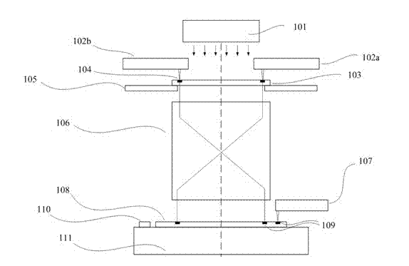
[0022] Such as figure 2 As shown, the existing lithography exposure device includes an exposure light source 101, left and right coaxial alignment detection devices 102a and 102b, a reticle 103, a mask mark 104, a mask table 105, a projection objective lens 106, and an off-axis alignment detection device 107 , the substrate 108, which may be glass, silicon wafer or other semiconductor materials, the substrate mark 109, the reference plate 110, the reference plate material here may be quartz, glass, silicon wafer or other materials, and the workpiece stage 111.

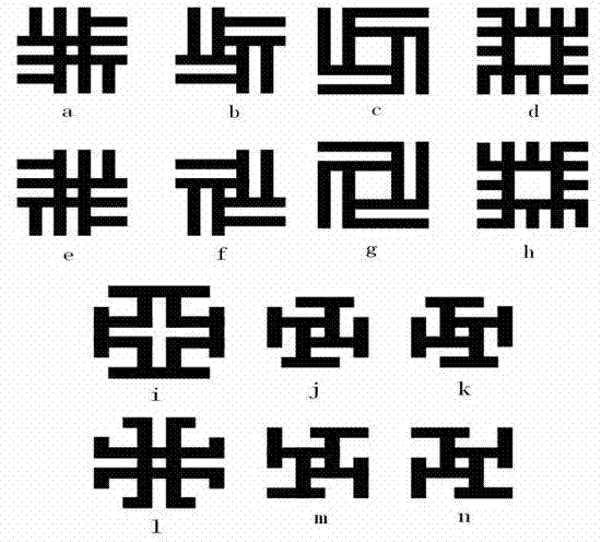
[0023] Such as image 3 Shown in a-n is a structural schematic diagram of a specific embodiment of the alignment mark of the present invention. The alignment marks a-n all meet the following characteristics at the same time: a. The alignment marks are integrally connected, that is, ...


PUM


Abstract

The invention provides an alignment mark for an exposure device. Simultaneously, the alignment mark is technically characterized in that a, the whole body of the alignment mark is connected, namely any line in the alignment mark has a crossed line; b, the alignment mark is a central symmetric figure; c, a peripheral outline (the crossed part of a mark periphery and a background) of the alignment mark is communicated (namely, any place along the outline is used as a starting point and the alignment mark always returns to the starting point no matter whether the alignment mark walks in a clockwise direction or an anticlockwise direction along the outline); d, the minimum line width and the gap size for forming the alignment mark are greater than the limiting resolution of a measurement lens of the alignment mark; e, no less than four horizontal or vertical lines for forming the alignment mark are arranged in each direction. The alignment mark disclosed by the invention has obvious outline characteristics and is the central symmetric figure, so that the resolution is improved; meanwhile, the lengths of the horizontal line and the vertical lines of the alignment mark are the same and the alignment precision is improved.

Description

technical field [0001] The invention relates to the technical field of semiconductor manufacturing, in particular to an alignment mark used in an alignment system of an exposure device of a lithography machine. [0002] Background technique [0003] The alignment system is a very important core subsystem of semiconductor lithography equipment, and its alignment accuracy often directly determines the overlay accuracy that semiconductor lithography equipment can achieve. The semiconductor lithography equipment projects the circuit pattern drawn on the reticle onto the surface of the exposure object such as a silicon wafer coated with a photosensitive material through an optical projection method. Then, the pattern transfer between the mask plate and the exposure object is realized through etching and other processes. Since chips are composed of multiple layers of circuits, integrated circuit chips usually require multiple exposures to complete. In order to ensure the precis...

Claims


Application Information

Patent Timeline
IPC IPC(8): G03F7/20G03F9/00
Inventor 陈跃飞徐兵杜荣贾翔
Owner SHANGHAI MICRO ELECTRONICS EQUIP (GRP) CO LTD
Why Eureka
Try Eureka