An alignment mark for an exposure device
A technology for aligning marks and exposure devices, which is applied in photolithography exposure devices, microlithography exposure equipment, optics, etc., can solve the problems of less signal volume, disconnected marks, and poor alignment accuracy, and achieve improved alignment. The effect of accurate precision and improved resolution
- Summary
- Abstract
- Description
- Claims
- Application Information
AI Technical Summary
Problems solved by technology
Method used
Image
Examples
Embodiment Construction
[0020] Specific embodiments of the present invention will be described in detail below in conjunction with the accompanying drawings.
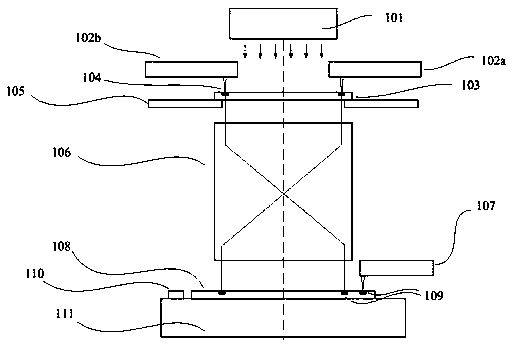
[0021] Such as figure 2 As shown, the existing lithography exposure device includes an exposure light source 101, left and right coaxial alignment detection devices 102a and 102b, a reticle 103, a mask mark 104, a mask stage 105, a projection objective lens 106, and an off-axis alignment detection device 107 , the substrate 108, which may be glass, silicon wafer or other semiconductor materials, the substrate mark 109, the reference plate 110, the reference plate material here may be quartz, glass, silicon wafer or other materials, and the workpiece stage 111.
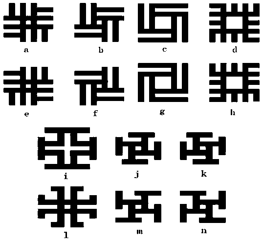
[0022] Such as image 3 Shown in a-n is a structural schematic diagram of a specific embodiment of the alignment mark of the present invention. The alignment marks a-n all meet the following characteristics at the same time: a. The alignment marks are integrally connected, that is, ...
PUM
 Abstract
Description
Claims
Application Information


