GaAs tunnel junction and preparation method thereof

A tunnel junction and doped layer technology, which is applied in the fields of final product manufacturing, sustainable manufacturing/processing, electrical components, etc., can solve the problems of low peak current not applicable to high-power concentrating multi-junction cells, etc., to improve photoelectric conversion efficiency, Effect of low impurity diffusion phenomenon and steep doping interface morphology

Active Publication Date: 2013-10-23
SUZHOU INST OF NANO TECH & NANO BIONICS CHINESE ACEDEMY OF SCI +1
View PDF4 Cites 7 Cited by
  • Summary
  • Abstract
  • Description
  • Claims
  • Application Information

AI Technical Summary

Problems solved by technology

[0005] The purpose of the present invention is to provide a GaAs tunnel junction with a novel dopant combination, the GaAs tunnel junction has high doping concentration and high peak current density, thereby improving the conversion efficiency of concentrating multi-junction solar cells to overcome the traditional molecular The GaAs tunnel junction grown by beam epitaxy with Si and Be as doping sources has serious diffusion, and the peak current is too low to be suitable for high-power concentrating multi-junction cells.

Method used


Image

  • GaAs tunnel junction and preparation method thereof
  • GaAs tunnel junction and preparation method thereof
  • GaAs tunnel junction and preparation method thereof

Examples


Embodiment Construction

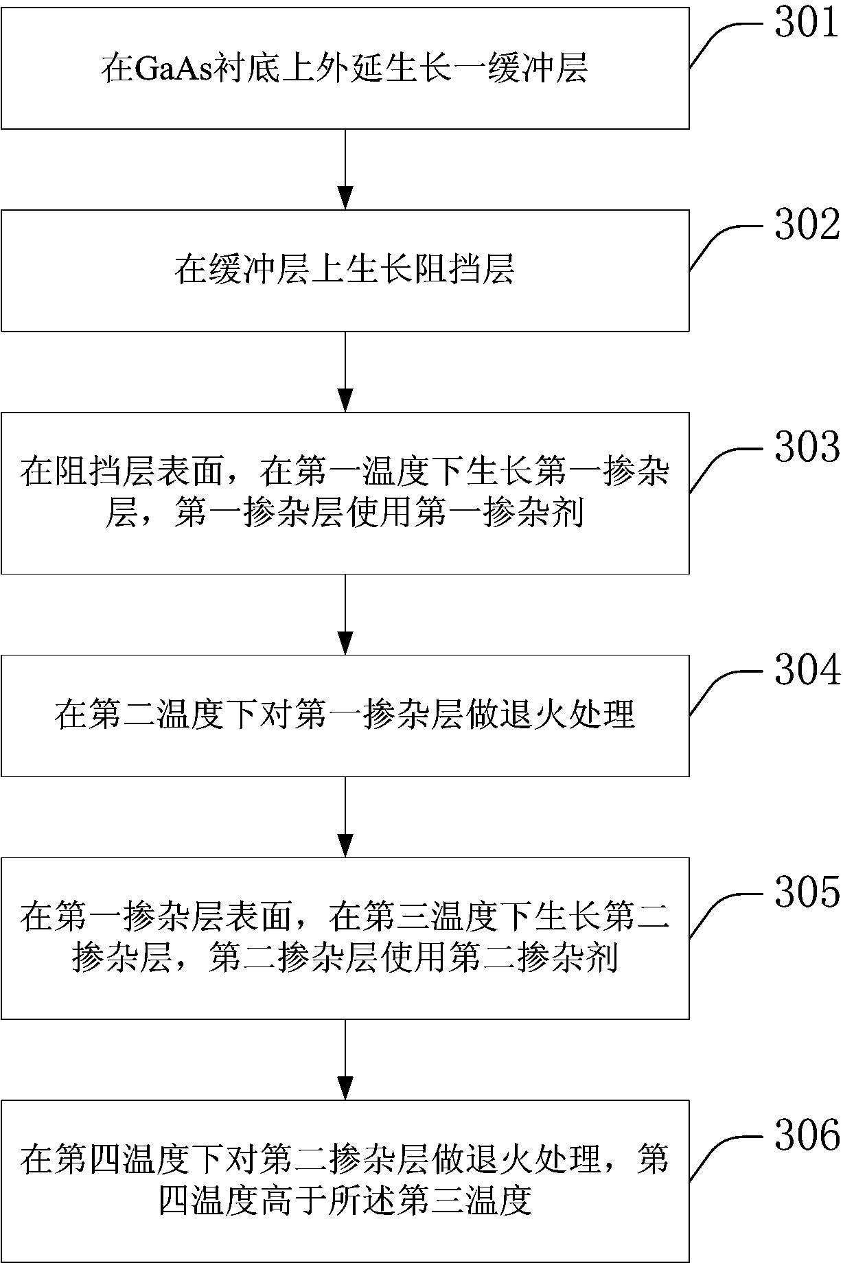
[0019] In order to make the present invention easier to understand, the GaAs tunnel junction and its preparation method of the present invention will be further described in detail below with reference to the accompanying drawings. However, the following descriptions and illustrations about the implementation modes and examples do not constitute any limitation to the protection scope of the present invention.

[0020] Firstly, a specific implementation manner of the GaAs tunnel junction of the present invention is given with reference to the accompanying drawings.

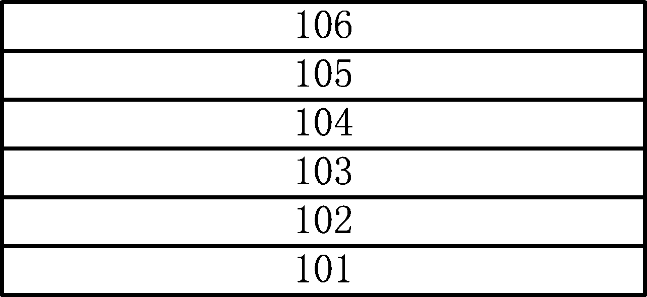
[0021] Reference attached figure 1 , the structural schematic diagram of the GaAs tunnel junction provided in this specific embodiment, and then the attached figure 1 The structure shown is described in detail.

[0022] This specific embodiment provides a GaAs tunnel junction, including: a barrier layer 103 , a first doped layer 104 and a second doped layer 105 sequentially disposed on the surface of a GaAs subst...


PUM

PropertyMeasurementUnit
current densityaaaaaaaaaa

Abstract

The invention provides a GaAs tunnel junction and a preparation method thereof. Excellent tunneling performance and a high peak current are achieved, the requirement for a high-power optically-focused multi-junction battery can be well met, and photoelectric conversion efficiency of the battery is promoted. The GaAs tunnel junction comprises a barrier layer, a first doped layer and a second doped layer, wherein the barrier layer, the first doped layer and the second doped layer are arranged on the surface of a GaAs substrate in sequence, and the GaAs substrate, the barrier layer and the first doped layer have the same conduction type. The GaAs tunnel junction is characterized in that if the first doped layer is in an n type and the first adulterant is Te, the second doped layer is in a p type, and the second adulterant is Mg; if the first doped layer is in a p type and the first adulterant is Mg, the second doped layer is in an n type, and the second adulterant is Te.

Description

technical field [0001] The invention relates to the field of semiconductor device structure and material growth, in particular to a GaAs tunnel junction and a preparation method thereof, and a multi-junction solar cell connected by the GaAs tunnel junction. Background technique [0002] In concentrating multi-junction solar cells, tunnel junctions must be used to realize the transport of photogenerated carriers between sub-cells. Under high concentration conditions, the photogenerated current will increase proportionally with the concentration ratio. Once the photogenerated current is greater than the peak current of the tunnel junction, the fill factor of the cell will decrease sharply, and the cell efficiency will decrease. Therefore, high-power concentrating multi-junction solar cells have an urgent requirement for high peak current of the tunnel junction, and the peak current of the tunnel junction is directly determined by the doping concentration and the diffusion stre...

Claims


Application Information

Patent Timeline
Patent Type & Authority Applications(China)
IPC IPC(8): H01L31/0352H01L31/18
CPCY02P70/50
Inventor 甘兴源郑新和吴渊渊王海啸王乃明陆书龙杨辉有持祐之内田史朗池田昌夫渡边知雅吉田浩野町一郎
Owner SUZHOU INST OF NANO TECH & NANO BIONICS CHINESE ACEDEMY OF SCI
Why Eureka
Try Eureka