Thin-film transistor and producing method thereof

A technology of thin-film transistors and manufacturing methods, which is applied in the direction of transistors, semiconductor/solid-state device manufacturing, and electrical components. The effect of stability and good interface adhesion

Inactive Publication Date: 2013-10-30
DONGGUAN MASSTOP LIQUID CRYSTAL DISPLAY +1
View PDF5 Cites 14 Cited by
  • Summary
  • Abstract
  • Description
  • Claims
  • Application Information

AI Technical Summary

Problems solved by technology

However, since the oxide channel layer is very sensitive to water, oxygen, acid etchant, etc., any environmental influence or process abnormality may cause abnormal electrical properties and uniformity of the device
In addition, the oxide channel layer will generate a photocurrent (photo current) under the irradiation of ultraviolet light, which will cause the lifetime (lifetime) and photoelectric characteristics of the thin film transistor to deteriorate.

Method used


Image

  • Thin-film transistor and producing method thereof
  • Thin-film transistor and producing method thereof
  • Thin-film transistor and producing method thereof

Examples


Embodiment Construction

[0048] Figure 1A to Figure 1F It is a schematic cross-sectional view of the manufacturing process of a thin film transistor according to an embodiment of the present invention.

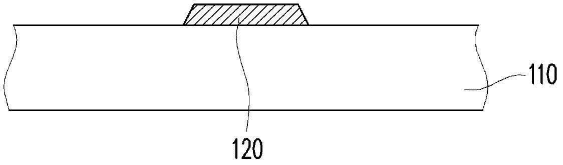
[0049] Please refer to Figure 1A , firstly, a substrate 110 is provided, and a gate 120 is formed on the substrate 110, wherein the gate 120 can be made of a metal stack or a single metal layer, and its material is, for example, aluminum or copper with good conductivity and other metals. Of course, according to actual needs, the grid 120 can be made of non-metal conductive material.

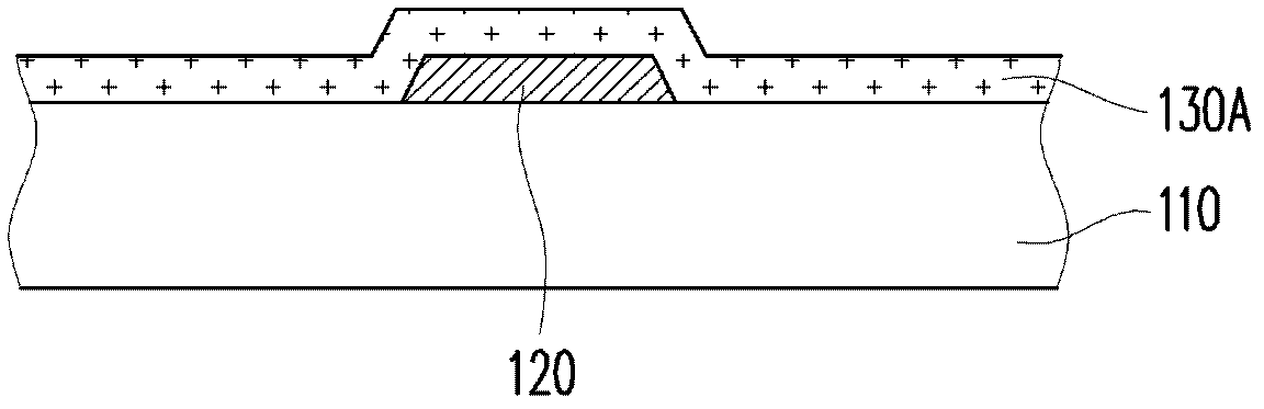
[0050] Please refer to Figure 1B , forming a gate insulating layer 130A on the substrate 110 , and making the gate insulating layer 130A cover the gate 120 . The material of the gate insulating layer 130A is, for example, an inorganic material (such as silicon oxide, silicon nitride, silicon oxynitride, silicon aluminum oxide, or a stacked layer of at least two of the above materials), an organic material, or a com...


PUM


Abstract

The invention provides a thin-film transistor and a producing method thereof. The thin-film transistor comprises a gate, an oxide channel layer, a gate insulation layer, a source, a drain and a dielectric layer. The gate is configured on a substrate. The oxide channel layer, which is configured on the substrate, stacks with the gate in an up and down manner. The material of the oxide channel layer comprises a metallic element and the content of the metallic element is in a gradient distribution along the depth direction of the oxide channel layer. The gate insulation layer is arranged between the gate and the oxide channel layer. The source and the drain which are parallelly configured are connected to the oxide channel layer. The dielectric layer is coated on the side, which is away from the substrate, of the source and the drain.

Description

technical field [0001] The present invention relates to a semiconductor element and its manufacturing method, and in particular to a thin film transistor and its manufacturing method. Background technique [0002] In recent years, with the rapid development of electronic technology, thin film transistor liquid crystal display (Thin Film Transistor Liquid Crystal Display, TFT LCD) with superior characteristics such as high image quality, good space utilization efficiency, low power consumption, and no radiation has gradually become the market choice. mainstream. [0003] With the requirement of large-area and high-resolution thin-film transistor liquid crystal displays, thin-film transistors must have high carrier mobility to shorten their charging and discharging time. In recent years, considering the problems of carrier mobility, flexibility and uniformity, the channel layer of the thin film transistor can be made of an oxide channel layer made of an oxide semiconductor la...

Claims


Application Information

Patent Timeline
Patent Type & Authority Applications(China)
IPC IPC(8): H01L29/786H01L21/34
Inventor 张惠喻游明璋邱家庆韩西容
Owner DONGGUAN MASSTOP LIQUID CRYSTAL DISPLAY
Why Eureka
Try Eureka