

Method for manufacturing graphere layer by laser
A graphene, laser light source technology, applied in graphene, nanotechnology for materials and surface science, semiconductor/solid-state device manufacturing, etc., can solve the problems of time-consuming, difficult to control graphene size, and high process temperature
- Summary
- Abstract
- Description
- Claims
- Application Information
AI Technical Summary
Problems solved by technology
Method used
Image

Examples
preparation example Construction
[0035] The method for preparing graphene provided by the present invention includes: providing a substrate; forming a metal layer on one side of the substrate; forming a carbon source substrate layer on the metal layer; providing a laser light source to irradiate the substrate passing through the substrate to the contact surface of the substrate and the metal layer to form a graphene layer; and providing an organic solvent and an acid solution to remove the carbon source substrate layer and the metal layer respectively.
[0036] Wherein, the laser light source is used to pass through the substrate and irradiate on the metal layer. Compared with the substrate and the carbon source substrate layer, the metal layer has a higher absorption rate of the laser light source (such as the wavelength of near-infrared light). Therefore, After the metal layer can effectively absorb the laser light energy, the temperature is raised to absorb the carbon atoms in the carbon source substrate la...
Embodiment 1
[0046] Embodiment 1: the making of unpatterned graphene
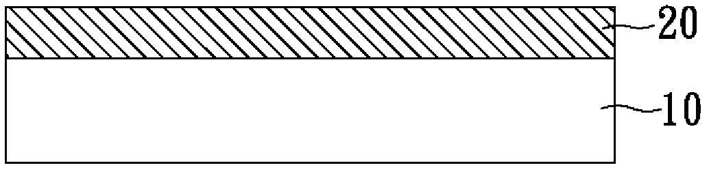
[0047] First, if Figure 1A As shown, a substrate 10 is provided. In this embodiment, the substrate 10 is a transparent glass substrate. On the substrate 10, a metal layer 20 is deposited on one side of the substrate 10. In this embodiment, the material of the metal layer 20 It is nickel and its thickness is about 100nm. In addition, the vapor deposition process conditions for forming the metal layer include: the degree of vacuum is 1×10 -5 torr, and the evaporation rate is
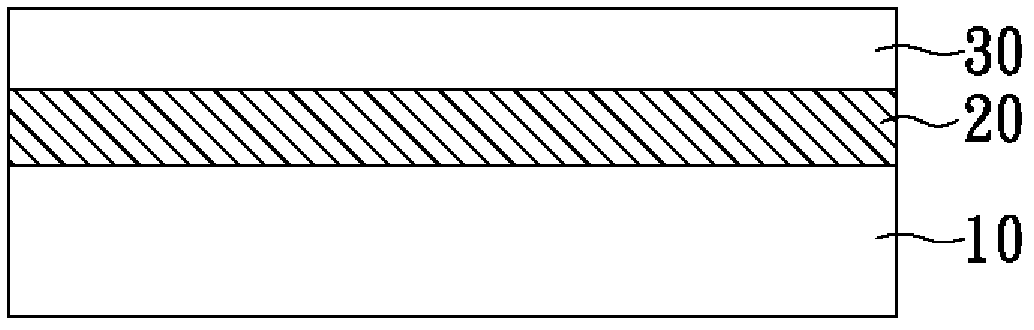
[0048] Next, if Figure 1B As shown, a carbon source substrate layer 30 is coated on the metal layer 20 . In this embodiment, the material of the carbon source substrate layer 30 is polymethyl methacrylate (PMMA), and its thickness is about 1000 nm. In addition, the coating process conditions for forming the carbon source substrate layer include: the rotational speed of the spin coater is 3000 rpm. At this time, a test piece of glass substr...
Embodiment 2
[0051] Example 2: Controlling the laser irradiation area to form patterned graphene
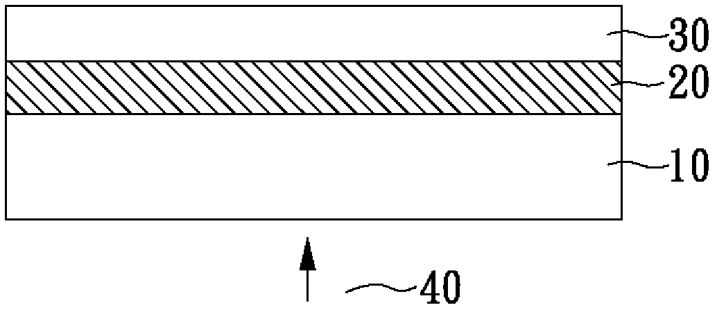
[0052] The material and preparation method of each layer in this embodiment 2 are the same as in embodiment 1, the difference lies in controlling the irradiation area of the laser light source 40, please refer to Figure 2A , where the A area is irradiated with laser light, while the B area is not irradiated with laser light. Generally speaking, metals have good thermal conductivity, and the temperature difference between the irradiated area and the non-irradiated area caused by local heating of the laser is not easy to appear, that is, in On a metal layer, in view of the high thermal conductivity of the metal, although the difference between the laser-irradiated and non-irradiated areas can not be clearly seen whether there is graphene or not, it can be obtained with different depths (that is, different thicknesses or layers) and graphite. Graphene with different quality, such as Figure ...
PUM
| Property | Measurement | Unit |
|---|---|---|
| thickness | aaaaa | aaaaa |
| thickness | aaaaa | aaaaa |
| wavelength | aaaaa | aaaaa |
Abstract
Description
Claims
Application Information