Graphene Enhanced Ingaas Infrared Detector

An infrared detector, graphene technology, applied in semiconductor devices, electrical components, circuits, etc., can solve the problems of difficulty in further improving mobility, affecting efficient absorption and conversion, and difficulty in growing InP single crystals, so as to improve photoelectric conversion efficiency. , the effect of low defect density and high relaxation

Inactive Publication Date: 2015-12-09
CHANGCHUN INST OF OPTICS FINE MECHANICS & PHYSICS CHINESE ACAD OF SCI
View PDF4 Cites 1 Cited by
  • Summary
  • Abstract
  • Description
  • Claims
  • Application Information

AI Technical Summary

Problems solved by technology

In addition, InP single crystal growth is difficult and fragile, and the mobility is difficult to further improve, and its device performance is close to the limit level
In addition, due to the introduction of the InP capping layer, the incident light will be reflected multiple times between multiple interfaces, which will weaken the light entering the absorbing layer, thus seriously affecting the efficient absorption and conversion of the optical signal by the InGaAs infrared detector.

Method used


Image

  • Graphene Enhanced Ingaas Infrared Detector

Examples


specific Embodiment approach 1

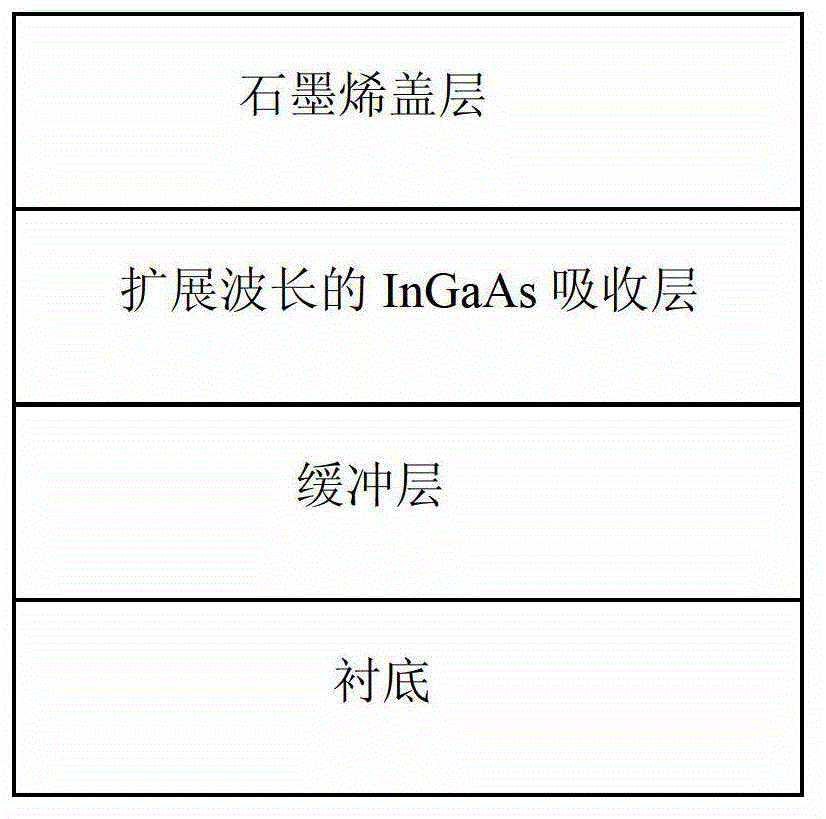
[0024] The structure of a graphene-enhanced InGaAs infrared detector with a cutoff wavelength of 2.6 μm is as follows: a thickness of about 1 μm is sequentially grown on an n-type GaAs substrate, and the Si doping concentration is 2×10 18 cm -3 n-type InAs 0.60 P 0.40 Buffer layer, continue to grow to a thickness of 2.5 μm, and a Si doping concentration of 8×10 16 cm -3 (lowly doped) n-type In 0.82 Ga 0.18 As absorption layer, and finally a single-layer p-type graphene cap layer is grown to form a pin detector structure.

[0025] In this embodiment, firstly, S-doped n-type GaAs is used as the substrate, and Si-doped InAs is grown on the GaAs substrate by the MOCVD system using a two-step method. 0.60 P 0.40 Buffer layer, first grow a layer of InAs with a thickness of about 100nm at a temperature of 450°C 0.60 P 0.40 , and then raise the temperature to 580°C, during the temperature rise process the buffer layer InAs 0.60 P 0.40 Anneal and recrystallize to release the...

specific Embodiment approach 2

[0026] A graphene-enhanced InGaAs infrared detector structure with a cutoff wavelength of 2.6 μm is: sequentially grown on an n-type InP substrate with a thickness of about 2 μm and a Si doping concentration of 2×10 18 cm -3 n-type In 0.82 al 0.18 As buffer layer, continue to grow to a thickness of 3.5 μm, and a Si doping concentration of 8×10 16 cm -3 (lowly doped) n-type In 0.82 Ga 0.18 As absorption layer, and finally grow multi-layer p-type graphene capping layer to form pin detector structure.

[0027]In this embodiment, firstly, S-doped n-type InP is used as the substrate, and Si-doped In is grown on the InP substrate by the MOCVD system using a two-step method. 0.82 al 0.18 As buffer layer, first grow a layer of about 200nm In at a temperature of 450°C 0.82 al 0.18 As, then raise the temperature to 580°C, the buffer layer In during the heating process 0.82 al 0.18 As is annealed and recrystallized to release the stress caused by the lattice mismatch and becom...


PUM


Abstract

The invention relates to a graphene enhancement type InGaAs infrared detector. The graphene enhancement type InGaAs infrared detector solves the technical problem that an existing infrared detector is narrow in detection range and high in dark current. According to the graphene enhancement type InGaAs infrared detector, a buffer layer, an InGaAs absorbing layer with wavelength extended and a graphene cover layer which grow sequentially on a substrate form a pin detector structure. The invention discloses a method for growing the mismatch buffer layer on the substrate in a two-step method. An InAlAs ternary system material or InAsP of an InGaAs material which is suitable for metallorganic chemical vapor deposition technology growth and convenient to control and enables forbidden bandwidth to be larger than extended wavelength is adopted and can effectively avoid mismatch dislocation and be suitable for a transparent buffer layer structure with light entering at the back. The method for utilizing graphene to serve as the cover layer of the InGaAs infrared detector to expand the detection range and reduce dark current is provided, detector performance is improved, and the graphene enhancement type InGaAs infrared detector has wide application prospect.

Description

technical field [0001] The invention relates to the application field of optoelectronic materials and devices, in particular to a wide-band graphene-enhanced InGaAs infrared detector using a graphene thin film as a cover layer. Background technique [0002] InGaAs detector is one of the most important short-wave infrared detectors at present. The narrow detection range and high dark current are the main problems restricting its development and application. In recent years, the device structure design of broadband InGaAs material has become the latest hot research direction in the field of international semiconductor photodetection research. The study found that since the InGaAs material is a full-component direct bandgap material, the application range of the detector can be effectively expanded by increasing the In component. However, increasing the In composition will inevitably lead to a lattice mismatch between the InGaAs material and the substrate, and when the mismatc...

Claims


Application Information

Patent Timeline
Patent Type & Authority Patents(China)
IPC IPC(8): H01L31/105H01L31/0352H01L31/0328
Inventor 张志伟缪国庆宋航蒋红黎大兵孙晓娟陈一仁李志明
Owner CHANGCHUN INST OF OPTICS FINE MECHANICS & PHYSICS CHINESE ACAD OF SCI
Why Eureka
Try Eureka