InGaAs (Indium Gallium Arsenide) or GaAs (Gallium Arsenide) infrared detector with wide detection bands

An infrared detector and band technology, applied in semiconductor devices, electrical components, circuits, etc., can solve problems such as lattice mismatch and detector performance degradation, and achieve the effects of improving detection rate, suppressing dark current, and improving quantum efficiency

Inactive Publication Date: 2013-11-06
CHANGCHUN INST OF OPTICS FINE MECHANICS & PHYSICS CHINESE ACAD OF SCI
View PDF3 Cites 6 Cited by
  • Summary
  • Abstract
  • Description
  • Claims
  • Application Information

AI Technical Summary

Problems solved by technology

[0006] The purpose of the present invention is to solve the problem that the lattice mismatch of existing InGaAs infrared detectors produce...

Method used


Image

  • InGaAs (Indium Gallium Arsenide) or GaAs (Gallium Arsenide) infrared detector with wide detection bands

Examples


Embodiment

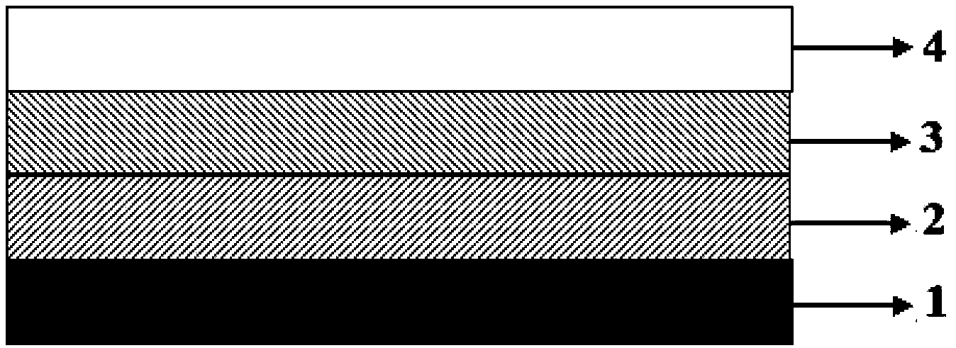
[0030] Step 1. First grow a layer of about 100 nm Si doping concentration of 2×10 on the S-doped n-type GaAs substrate 1 at a temperature of 450° C. by using the MOCVD system. 18 cm -3 InAs 0.60 P 0.40 Buffer layer 2, then raise the temperature to 580°C, during the heating process InAs 0.60 P 0.40 The buffer layer 2 is annealed and recrystallized to release the stress caused by the lattice mismatch and become the interface for the next growth. The thickness of the buffer layer 2 is 1 μm;

[0031] Step 2: After keeping the temperature at 550° C. for 3-5 minutes, grow a layer of 3 μm Si doping concentration on the above interface with a doping concentration of 8×10 16 cm -3 n-type In 0.82 Ga 0.18 As absorption layer 3;

[0032] Step 3, growing a Be doping concentration of 1 μm on the absorber layer 3 with a concentration of 2×10 17 cm -3 p-type In 0.82 Al 0.18 The As cap layer 4 is used to obtain an InGaAs / GaAs infrared detector with a pin structure and a wide detect...


PUM

PropertyMeasurementUnit
Thicknessaaaaaaaaaa
Thicknessaaaaaaaaaa
Doping concentrationaaaaaaaaaa

Abstract

The invention discloses an InGaAs (Indium Gallium Arsenide) or GaAs (Gallium Arsenide) infrared detector with wide detection bands and belongs to the field of optoelectronic materials and devices. The InGaAs or GaAs infrared detector solves the problem that the performance of the existing InGaAs infrared detectors decreases obviously due to the fact that defects are produced by lattice mismatch. The InGaAs or GaAs infrared detector comprises a buffering layer, an absorbing layer and a covering layer which are grown on a GaAs substrate sequentially; the buffering layer is InAsP (Indium Arsenide Phosphorus) doped with Si (Silicon) and the thickness of the buffering layer is 0.5 to 1.5 microns; the absorbing layer is In0.82Ga0.18As with low doped Si and the thickness of the absorbing layer is 2.5 to 3.5 microns; the covering layer is InAlAs (Indium Aluminum Arsenide) doped with Be (Beryllium) and the thickness of the covering layer is 0.5 to 1.5 microns. The InGaAs or GaAs infrared detector with the wide detection bands has the structure which is high in quantum efficiency and high in detection rate and can meet the requirements of front light entering, back light entering and flip chip packaging.

Description

technical field [0001] The invention relates to an InGaAs / GaAs infrared detector with a wide detection band, belonging to the field of optoelectronic materials and devices. Background technique [0002] Detectors made of InGaAs materials have the advantages of high sensitivity, fast response, good radiation resistance, and room temperature operation, making them ideal materials for space remote sensing in the near-infrared band. For detectors used in space remote sensing, the focus of research is to suppress noise, reduce the dark current of the device, and improve the detection rate. [0003] At present, in the structural design of InGaAs infrared detectors, especially in semiconductor photovoltaic infrared detectors, pin structures are used, including n-type substrates, absorbing layers i-layers are InGaAs with different components, p-type capping layers, positive and negative metals electrode. The InGaAs material is a full-component direct bandgap material, and the appl...

Claims


Application Information

Patent Timeline
IPC IPC(8): H01L31/105H01L31/0304H01L31/0352
Inventor 张志伟缪国庆宋航蒋红黎大兵孙晓娟陈一仁李志明
Owner CHANGCHUN INST OF OPTICS FINE MECHANICS & PHYSICS CHINESE ACAD OF SCI
Why Eureka
Try Eureka