A Superlattice Waveguide Semiconductor Laser Structure

A superlattice and laser technology, applied in the structure of optical waveguide semiconductors, can solve the problems of electron and hole electrical confinement imbalance, optical field distribution optimization, etc., to optimize the effective refractive index, improve electrical characteristics, increase The effect of output power

Inactive Publication Date: 2016-08-31
CHANGCHUN UNIV OF SCI & TECH
View PDF2 Cites 0 Cited by
  • Summary
  • Abstract
  • Description
  • Claims
  • Application Information

AI Technical Summary

Problems solved by technology

[0004] The main purpose of this method is to provide a superlattice waveguide semiconductor laser structure, to solve the problem of unbalanced electron and hole electrical confinement in semiconductor lasers, and the optimization of optical field distribution after using heterogeneous waveguides

Method used


Image

  • A Superlattice Waveguide Semiconductor Laser Structure
  • A Superlattice Waveguide Semiconductor Laser Structure
  • A Superlattice Waveguide Semiconductor Laser Structure

Examples


specific Embodiment

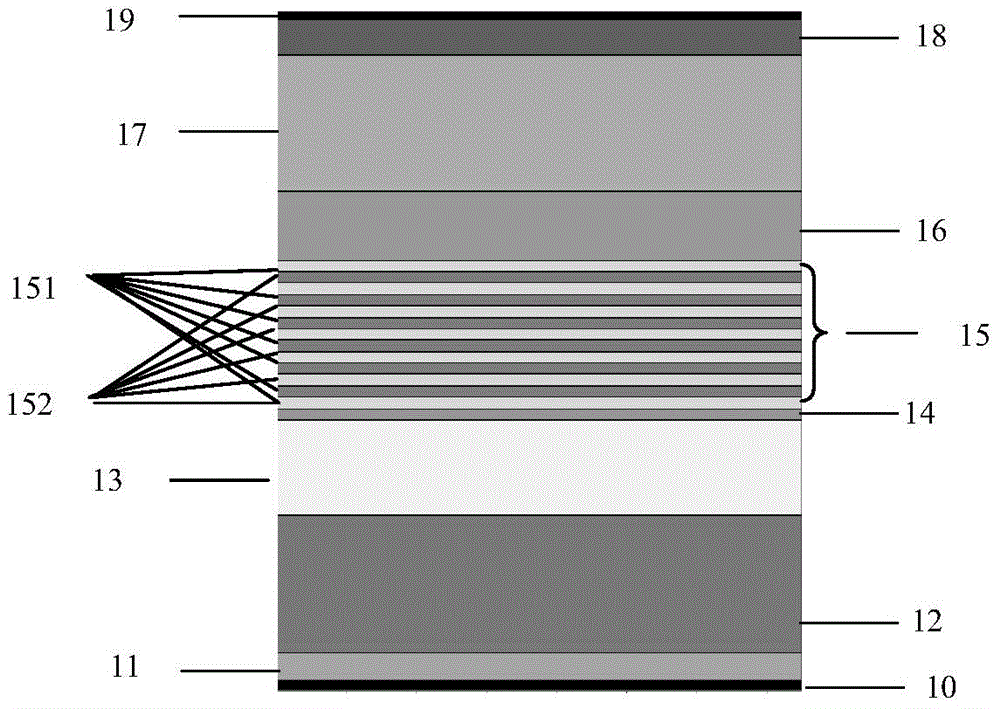
[0029] Combine below figure 1 The structural details of a superlattice waveguide semiconductor laser according to a specific embodiment of the present invention will be described in detail.

[0030] refer to figure 1 , the present invention is a superlattice waveguide semiconductor laser structure, comprising:

[0031] A substrate 10 is an N-type GaAs material of (100) plane, and the substrate 10 is used to epitaxially grow each layer of material of the laser thereon;

[0032] A buffer layer 11, made of N-GaAs material, the buffer layer 11 is fabricated on the substrate 10, and is mainly used to adjust the lattice fit;

[0033] An N-type lower confinement layer 12, which is N-In 1-x Ga x As y P 1-y material, the N-type lower confinement layer 12 is fabricated on the buffer layer 11;

[0034] An N-type lower waveguide layer 13, which is N-In 1-x Ga x As y P 1-y material, the lower waveguide layer 13 is made on the lower confinement layer 12;

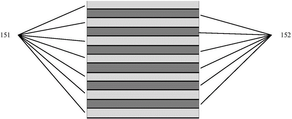
[0035] A quantum well ...

Embodiment

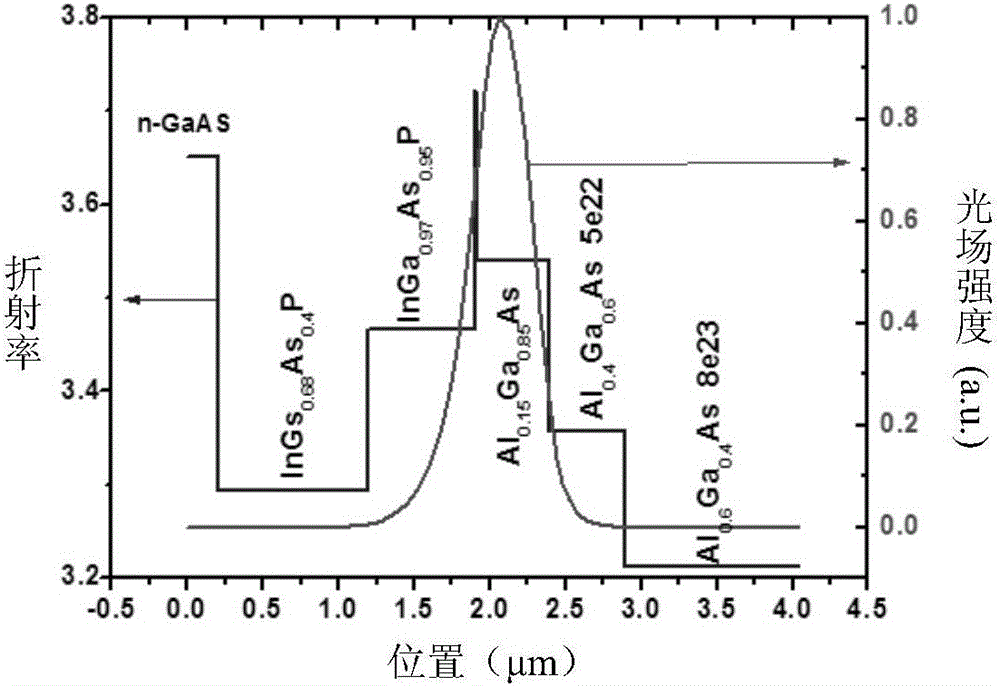
[0044] This embodiment adopts figure 1 The structure shown shows the laser light field distribution under the modulation of the superlattice waveguide. The substrate of the structure is N-type GaAs material, and the material and thickness of each layer of the structure from bottom to top are as follows:

[0045] The substrate material and thickness are GaAs, 0.2 μm; the lower confinement layer material and thickness are In 0.32 Ga 0.68 As 0.4 P 0.6 ,1μm; the material and thickness of the lower waveguide layer are In 0.03 Ga 0.97 As 0.95 P 0.05 ,0.7μm; quantum well layer material and thickness are In 0.3 Ga 0.7 As, 9nm; the material and thickness of the upper superlattice waveguide with low Al components are Al 0.15 Ga 0.85 As, 8nm; the material and thickness of the upper superlattice waveguide with high Al composition are Al 0.4 Ga 0.6 As, 10nm; the material and thickness of the upper waveguide layer are Al 0.4 Ga 0.6 As, 0.8μm; the material and thickness of the...


PUM


Abstract

The invention belongs to the technical field of photoelectrons, and relates to a super-lattice waveguide semiconductor laser structure. The super-lattice waveguide semiconductor laser structure sequentially comprises, from bottom to top, an N-type gallium arsenide substrate, an N-type gallium arsenide buffering layer, an N-type lower limiting layer, an N-type lower waveguide layer, a quantum well layer, a P-type upper super-lattice waveguide layer, a P-type upper waveguide layer, a P-type upper limiting layer, a transition layer and an electrode contacting layer. The substrate is used for epitaxially growing various layers of materials of a laser, the N-type gallium arsenide buffering layer is mainly used for adjusting the adaption degree of a lattice, the N-type lower limiting layer is an InGaAsP quaternary compound material and used for limiting downward leakage of a light filed, the N-type lower waveguide layer is an InGaAsP quaternary compound material and used for enhancing the limitation to the light field mode, the quantum well layer (an active area material) is an InGaAs single quantum well, the P-type upper super lattice waveguide layer is an AlGaAs material and used for modulating the waveguide refractive index, the P-type upper waveguide layer is an AlGaAs material and used for enhancing the limitation to the light field mode, the P-type upper limiting layer is an AlGaAs material and used for limiting upward leakage of the light field, the transition layer is a GaAs material, and the electrode contacting layer is a GaAs material and used for forming an upper electrode with metal.

Description

technical field [0001] The invention relates to the technical field of semiconductor optoelectronic devices, in particular to a superlattice waveguide semiconductor laser structure. Background technique [0002] Semiconductor lasers are widely used in material processing, medical, information storage and military, such as laser processing, laser medical treatment, laser annealing and laser guidance. Since the birth of semiconductor lasers, research institutions and units at home and abroad have conducted detailed research on them from the aspects of epitaxial materials, structural design, and manufacturing technology. The research and application of high-power semiconductor lasers with high conversion efficiency, low loss, high stability, and high beam quality have gradually matured. With the deepening of research, the performance of the laser has been improved. However, there are still many unsatisfactory aspects of semiconductor lasers. For example, semiconductor lasers ...

Claims


Application Information

Patent Timeline
Patent Type & Authority Patents(China)
IPC IPC(8): H01S5/20
Inventor 李特张月李再金郝二娟邹永刚芦鹏曲轶刘国军马晓辉
Owner CHANGCHUN UNIV OF SCI & TECH
Why Eureka
Try Eureka