Composite flexible transparent electrode of copper nanowires and poly (3, 4-ethylenedioxy group thiophene)-poly (styrene sulfoacid) and manufacturing method thereof

A technology of copper nanowires and transparent electrodes, which is applied in cable/conductor manufacturing, circuits, electrical components, etc., can solve problems such as poor adhesion, large roughness, and easy oxidation of copper nanowire films, and achieve good application value Effect

Inactive Publication Date: 2013-12-11
NANJING UNIV OF POSTS & TELECOMM
View PDF11 Cites 30 Cited by
  • Summary
  • Abstract
  • Description
  • Claims
  • Application Information

AI Technical Summary

Problems solved by technology

The present invention proposes a flexible transparent electrode formed by compounding copper nanowire film and PEDOT:PSS film, which is characterized in that this composite structure effectively solves the problems of easy oxidation, large roughness and poor adhesion of copper nanowire film, and Exhibiting a synergistic effect in conduction, the composite film is more conductive than copper nanowire transparent conductive film or PEDOT:PSS transparent conductive film

Method used


Image

  • Composite flexible transparent electrode of copper nanowires and poly (3, 4-ethylenedioxy group thiophene)-poly (styrene sulfoacid) and manufacturing method thereof
  • Composite flexible transparent electrode of copper nanowires and poly (3, 4-ethylenedioxy group thiophene)-poly (styrene sulfoacid) and manufacturing method thereof
  • Composite flexible transparent electrode of copper nanowires and poly (3, 4-ethylenedioxy group thiophene)-poly (styrene sulfoacid) and manufacturing method thereof

Examples


Embodiment 1

[0020] (1) Remove the PET outer protective film.

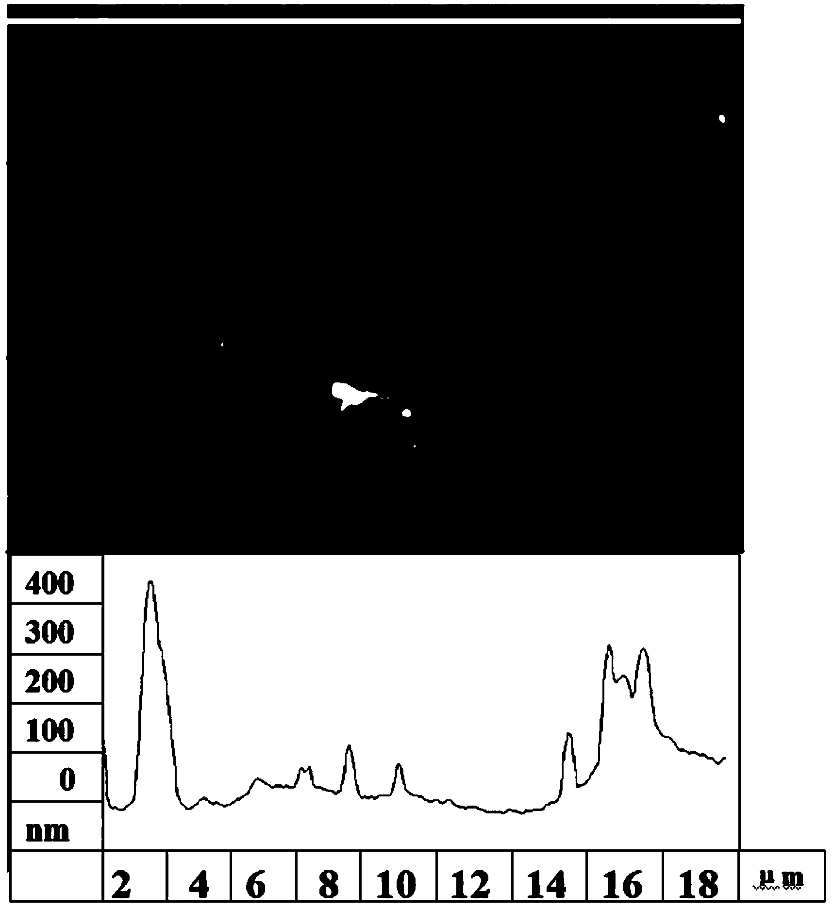
[0021] (2) Copper nanowires are evenly dispersed in a solvent, and a copper nanowire film is prepared on a clean substrate by spin coating.

[0022] (3) The PEDOT:PSS film was transferred by spin coating to be superimposed on the copper nanowire film, wherein the mass ratio of copper nanowires and PEDOT:PSS was 80 / 20. Place the substrate in an environment at 120°C for 30 minutes to remove the residual solvent in the overlay.

[0023] (4) Carry out thermal curing and pressure treatment on the laminated flexible substrate and conductive layer. Form substrates (flexible electrodes) for flexible optoelectronic devices.

[0024] (5) The light transmittance of the substrate (flexible electrode) for testing flexible optoelectronic devices is 85%, and the square resistance of the film is 30Ω / sq.

Embodiment 2

[0026] (1) Remove the PET outer protective film.

[0027] (2) Copper nanowires are evenly dispersed in a solvent, and a copper nanowire film is prepared on a clean substrate by spin coating.

[0028] (3) The PEDOT:PSS film was transferred by spraying method, so that it was superimposed on the copper nanowire film, and the mass ratio of copper nanowire and PEDOT:PSS was 83 / 17. Place the substrate in an environment at 120°C for 30 minutes to remove the residual solvent in the overlay.

[0029] (4) Carry out thermal curing and pressure treatment on the laminated flexible substrate and conductive layer. Form substrates (flexible electrodes) for flexible optoelectronic devices.

[0030] (5) The light transmittance of the substrate (flexible electrode) for testing flexible optoelectronic devices is 83%, and the film resistance is 50Ω / sq.

Embodiment 3

[0032] (1) Remove the PET outer protective film.

[0033] (2) Copper nanowires are evenly dispersed in a solvent, and a copper nanowire film is prepared on a clean substrate by spin coating.

[0034] (3) The PEDOT:PSS film was transferred by the self-assembly method to be superimposed on the copper nanowire film, wherein the mass ratio of copper nanowires and PEDOT:PSS was 90 / 10. Place the substrate in an environment at 120°C for 30 minutes to remove the residual solvent in the overlay.

[0035] (4) Carry out thermal curing and pressure treatment on the laminated flexible substrate and conductive layer. Form substrates (flexible electrodes) for flexible optoelectronic devices.

[0036] (5) The light transmittance of the substrate (flexible electrode) for testing flexible optoelectronic devices is 90%, and the film resistance is 700Ω / sq.


PUM

PropertyMeasurementUnit
thicknessaaaaaaaaaa
thicknessaaaaaaaaaa
transmittivityaaaaaaaaaa

Abstract

The invention discloses a flexible transparent electrode and a manufacturing method of the flexible transparent electrode. The flexible transparent electrode is formed by compositing copper nanowires and poly (3, 4-ethylenedioxy group thiophene)-poly (styrene sulfoacid) (PEDOT: PSS) to form a conducting layer and attaching the conducting layer to a transparent polymer substrate. The flexible transparent electrode and the manufacturing method of the flexible transparent electrode solve the problems that a copper nanowire film is poor in stability and large in roughness, and the combination force between the copper nanowire film and the flexible substrate is poor. A copper nanometer wire and PEDOT: PSS composite film has the advantages of being high in conductivity, high in light transmittance, good in flexibility and the like. The obtained flexible transparent electrode has good application value in image sensors, solar cells, liquid crystal displays, organic electroluminescence displays, touch screen panels and the like.

Description

technical field [0001] The invention relates to a copper nanowire and conductive polymer composite flexible transparent electrode and a preparation method thereof. Background technique [0002] Transparent conductive films are important components of many optoelectronic devices, such as flat panel displays, organic solar cells, organic light-emitting diodes (OLEDs), smart windows, etc. Indium tin oxide (ITO) has become the main material for transparent conductive films due to its high electrical conductivity and light transmittance. However, ITO also has some disadvantages, such as the rising price of raw material indium and the high cost of preparation. In addition, once the ITO material is bent, its electrical conductivity will be greatly reduced. Therefore, the development of new materials that can replace ITO has become an extremely important research topic. New materials represented by conductive polymers, metal nanomaterials, carbon nanotubes and graphene show good d...

Claims


Application Information

Patent Timeline
Patent Type & Authority Applications(China)
IPC IPC(8): H01B1/12H01B1/02H01B5/14H01B13/00
Inventor 马延文陈剑宇周伟新张自强濮丹凤黄维
Owner NANJING UNIV OF POSTS & TELECOMM
Why Eureka
Try Eureka