
Array substrate, manufacturing method of array substrate, and display device

An array substrate and electrode layer technology, applied in the field of organic electroluminescent display, can solve the problems of high manufacturing process and difficulty, deviation of luminous color, limited types of materials, etc., and achieve the goal of improving luminous efficiency, enhancing luminous efficiency, and improving light extraction efficiency Effect

Active Publication Date: 2013-12-11
BOE TECH GRP CO LTD
View PDF4 Cites 18 Cited by
  • Summary
  • Abstract
  • Description
  • Claims
  • Application Information

AI Technical Summary

Problems solved by technology

Among them, through the improvement of the performance of the material, the current device with an internal quantum efficiency close to 100% can be realized theoretically, but the types of materials are very limited; and the loss of the waveguide mode can be reduced by fabricating the surface microstructure on the ITO electrode, and the photonic crystal or micro The lens array is attached to the glass substrate to reduce total internal reflection, the cathode is fabricated to reduce its surface plasmon loss, and the optical microcavity structure is used. Although these technologies can greatly increase the light extraction efficiency of the device, the photonic crystal and the cathode Forming periodic or quasi-periodic microstructure patterns on the surface, which often uses nanophotographic technology, the preparation process and difficulty are relatively large
However, the microcavity effect is likely to cause the deviation of the luminous color and the narrowing of the viewing angle.

Method used


Image

  • Array substrate, manufacturing method of array substrate, and display device
  • Array substrate, manufacturing method of array substrate, and display device
  • Array substrate, manufacturing method of array substrate, and display device

Examples


Embodiment 1

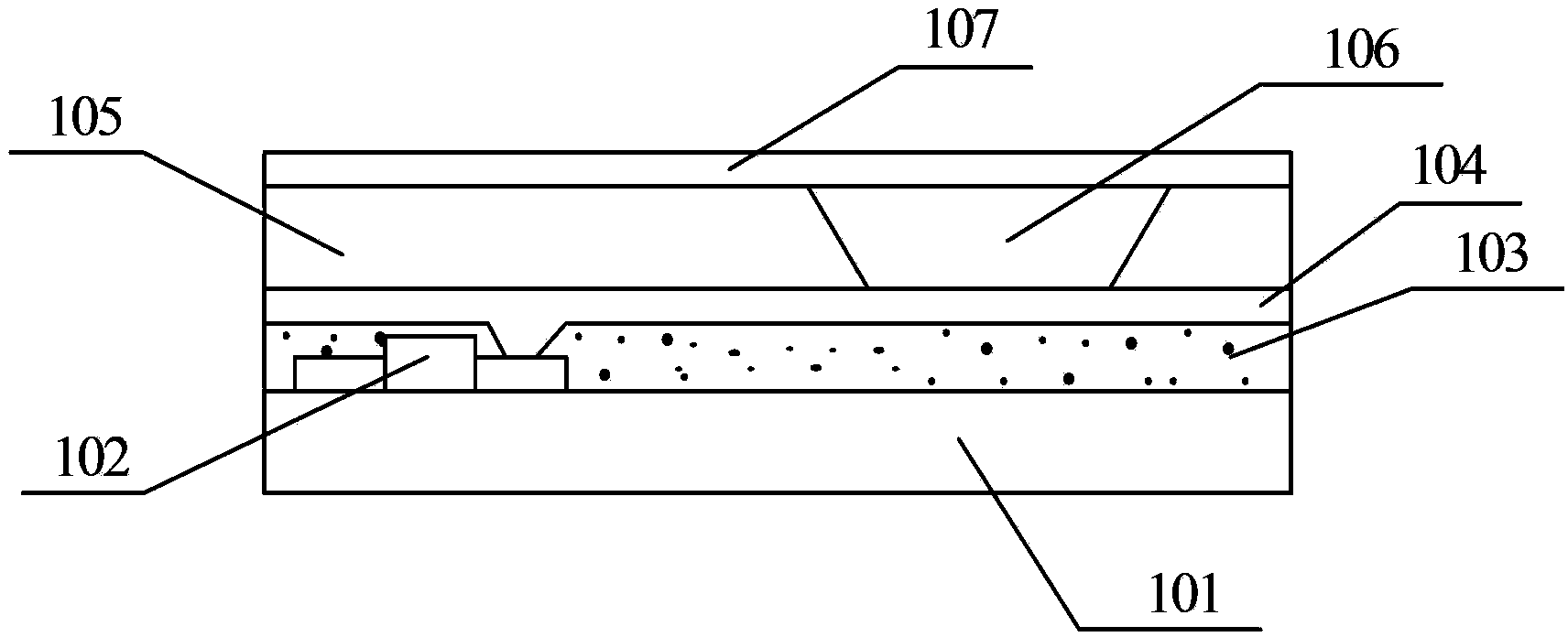
[0033] combine image 3 , this embodiment provides an array substrate, which includes an organic electroluminescent device, and the organic electroluminescent device includes: a first electrode layer 104, a second electrode layer 107, and The light-emitting layer 106 between 107, wherein the first electrode layer 104 is a transparent electrode layer, which is disposed on the planarization layer 103 doped with metal micro-nano particles q.

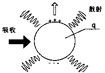
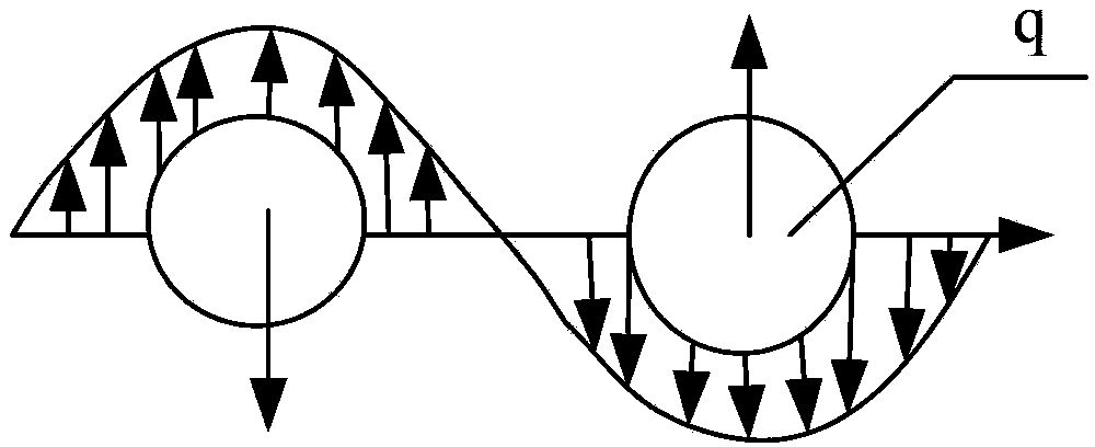
[0034] The planarization layer 103 below the transparent electrode layer of the organic electroluminescent device of the array substrate in this embodiment is doped with metal micro-nano particles q, and the surface plasmon resonance effect of the metal micro-nano particles q is used to enhance organic electroluminescence The luminous efficiency of the device is improved, thereby enhancing the light extraction rate of the array substrate.

[0035] It should be noted that surface plasmons (surface plasmons; SPs) refer to the electron densit...

Embodiment 2

[0050] This embodiment provides a display device, which includes the array substrate described in Embodiment 1. The display device can be any device with a display function such as a mobile phone, a tablet computer, a television, a monitor, a notebook computer, a digital photo frame, a navigator, etc. product or part.

[0051] The display device of this embodiment has the array substrate in Embodiment 1, so it has better luminous efficiency and better visual effect.

[0052] Certainly, the display device of this embodiment may also include other conventional structures, such as a power supply unit, a display driving unit, and the like.

Embodiment 3

[0054] This embodiment provides a method for preparing an array substrate, which includes the following steps:

[0055] Step 1, forming a thin film transistor 102 on the substrate 101 through a patterning process. Wherein, the thin film transistor 102 may be a top-gate type or a bottom-gate type.

[0056] Of course, gate lines, data lines, etc. can also be formed at the same time, and the driving of the thin film transistors can be 2T1C, etc.

[0057] Step 2, forming a planarization layer 103 doped with metal micro-nano particles q on the substrate 101 on which the thin film transistor 102 is formed.

[0058] Wherein, the preparation of the planarization layer 103 doped with metal micro-nano particles q can adopt the following method;

[0059] Method 1, such as Figure 5 As shown in the schematic diagram of the structure, a first planarization layer 1031 is first deposited on the prepared thin film crystal substrate 101, and then a 2nm thick gold layer is plated on its surf...


PUM


Abstract

The invention provides an array substrate, a manufacturing method of the array substrate, and a display device and belongs to the technical field of organic electroluminescence display. The array substrate, the manufacturing method of the array substrate, and the display device can solve the problem that an existing array substrate is low in light out-coupling efficiency. The array substrate comprises an organic electroluminescence device, wherein the organic electroluminescence device comprises a first electrode layer, a second electrode layer, and a luminescent layer arranged between the first electrode layer and the second electrode layer, and the first electrode layer is a transparent electrode layer and is arranged on a planarization layer mingled with metal micro-nano particles.

Description

technical field [0001] The invention belongs to the technical field of organic electroluminescence display, and in particular relates to an array substrate, a preparation method thereof, and a display device. Background technique [0002] The basic structure of an organic electroluminescent device (OLED) includes: an anode layer, a cathode layer, and a "light-emitting layer" sandwiched between the anode layer and the cathode layer, wherein the light-emitting layer is one or more organic layers. Under the action of an applied voltage, electrons and holes are injected into the organic layer from the cathode direction and the anode direction respectively, then migrate and meet and recombine in the "light-emitting layer" to generate excitons, and the energy of the excitons decays in the form of light, that is, radiation sold out. [0003] Organic electroluminescent devices can be divided into top emission type (Top emission) and bottom emission type (Bottom emission) according ...

Claims


Application Information

Patent Timeline
Patent Type & Authority Applications(China)
IPC IPC(8): H01L27/32H01L51/52H01L21/77
CPCH10K59/124H10K2102/331H10K59/877H10K50/816H10K50/828H10K50/854H10K59/123H10K71/00H10K59/1201H10K2102/00H10K2102/103
Inventor 代青刘则
Owner BOE TECH GRP CO LTD
Learn More