Low-differential-loss low-phase-shift high-integration-level five-level marching type ultra-wide-band numerical control attenuator

A high-integration, low-phase-shift technology, applied in the field of communications, can solve the problems of reducing system integration, occupancy, and chip area increase, and achieve the effects of improving integration, reducing manufacturing costs, and reducing chip area

Active Publication Date: 2013-12-11
XIDIAN UNIV
View PDF6 Cites 18 Cited by
  • Summary
  • Abstract
  • Description
  • Claims
  • Application Information

AI Technical Summary

Problems solved by technology

The disadvantage of the digitally controlled attenuator circuit disclosed in the patent application documents is that the reference state and the attenuation state of the attenuator are two signal paths respectively, which occupy a large chip area and reduce the integration level of the system chip integrated with this circuit The SPDT switch will not only increase the complexity of the circuit structure and occupy a large chip area, but also its large parasitic capacitance will introduce large insertion loss and additional phase shift in the signal path when the frequency is high
Although the numerically controlled attenuator disclosed in this patent application document has low insertion loss and additional phase shift, there are still shortcomings: the high electron mobility transistor of the GaAs process is used in the numerically controlled attenuator as the switch between different attenuation module states Control switch, high production cost, low yield; GaAs process is not compatible with the current silicon process used in VLSI manufacturing, which is not conducive to the realization of single-chip integrated ultra-wideband radio frequency microwave system
The disadvantages of the numerically controlled attenuator circuit disclosed in the patent application documents are: two signal channels with a numerically controlled attenuator structure are used for signal processing, which increases the complexity of the circuit structure and doubles the occupied chip area. greatly reduces the chip integration of the circuit
The numerically controlled attenuator also uses GaAs process field effect transistors as control switches. Although the attenuation range is large and the attenuation accuracy is high, there are still shortcomings: the overall numerically controlled attenuator is composed of multiple independent attenuation modules cascaded. , takes up a large chip area, and when used for ultra-wideband system integration, it will reduce the integration level of the system

Method used


Image

  • Low-differential-loss low-phase-shift high-integration-level five-level marching type ultra-wide-band numerical control attenuator
  • Low-differential-loss low-phase-shift high-integration-level five-level marching type ultra-wide-band numerical control attenuator
  • Low-differential-loss low-phase-shift high-integration-level five-level marching type ultra-wide-band numerical control attenuator

Examples


Embodiment 1

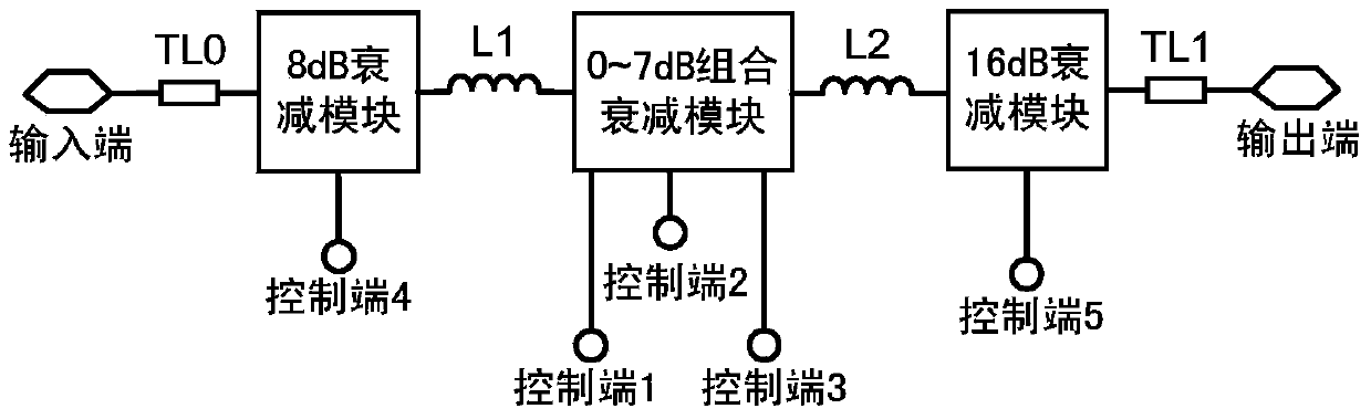
[0038] Embodiment 1: working state of the present invention. Embodiment 1 of the present invention is controlled by five digital signals respectively, and the different level states of the control signals input to each control terminal and the corresponding signal amplitude attenuation states are shown in the following table.

[0039]

[0040] In the table, 0 means low level and 1 means high level. It can be seen from the above table that the present invention changes the high and low level state of the input control signal through the control terminal 1, the control terminal 2, the control terminal 3, the control terminal 4 and the control terminal 5 respectively, stepping in 12.5-18GHz with a length of 1dB Within the operating frequency range and the attenuation range of 0 ~ 31dB, 32 states of low drop loss and low phase shift signal amplitude attenuation are realized.

Embodiment 2

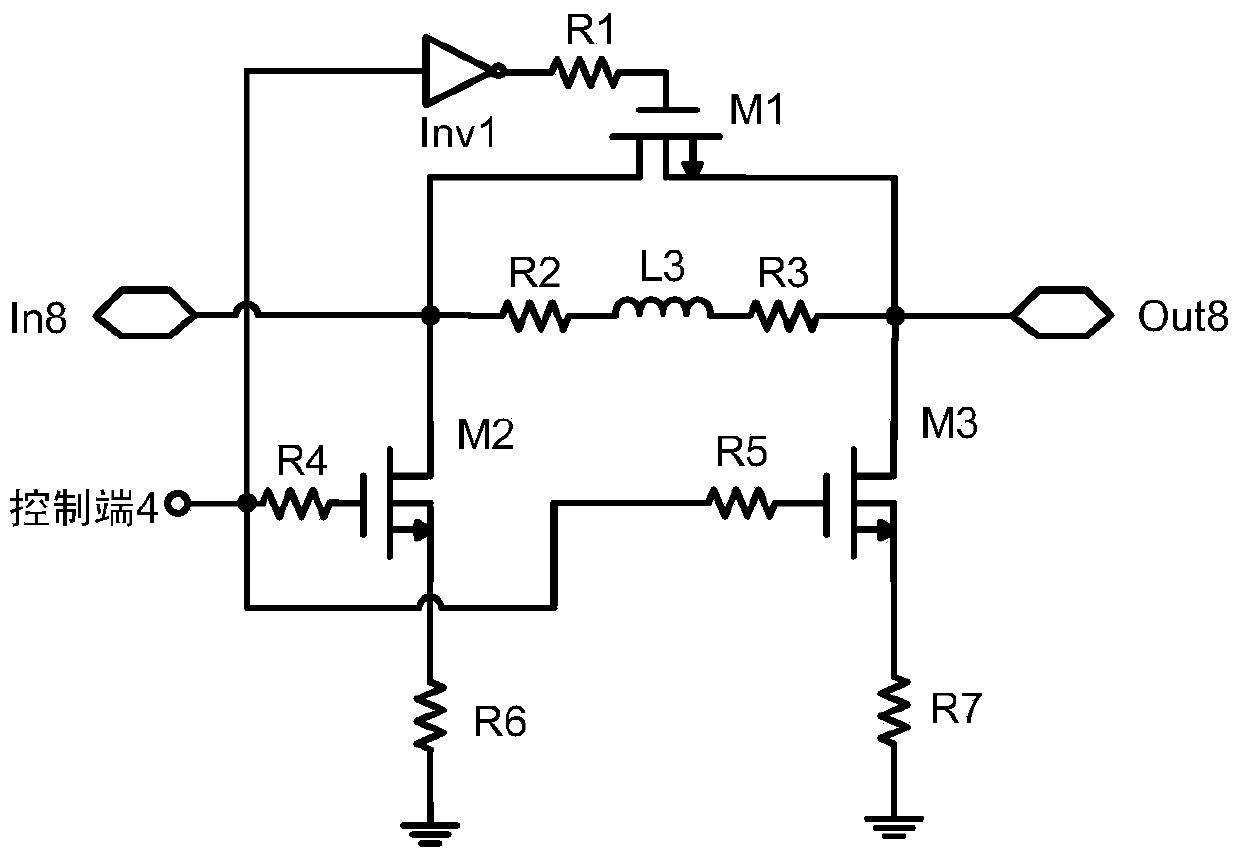
[0041] Embodiment 2: the working process of the 8dB attenuation module of the present invention. Embodiment 2 of the present invention adopts Figure 6 The MOS transistor switch shown is used as the control switch of the series branch and the parallel branch, and an additional phase shift compensation inductance network is used for phase shift compensation to achieve signal amplitude attenuation while reducing the additional phase shift of the output signal relative to the input signal . The 8dB attenuation module can be controlled at the control terminal 4 by a digital signal. When the input of the control terminal 4 is at a low level, the input of the inverter Inv1 is at a low level, the output of the inverter Inv1 is at a high level, the switch MOS transistor M1 is turned on, and both the switch MOS transistor M2 and the switch MOS transistor M3 are turned off. The 8dB attenuation module is in reference state. When the input of the control terminal 4 is at a high level, ...

Embodiment 3

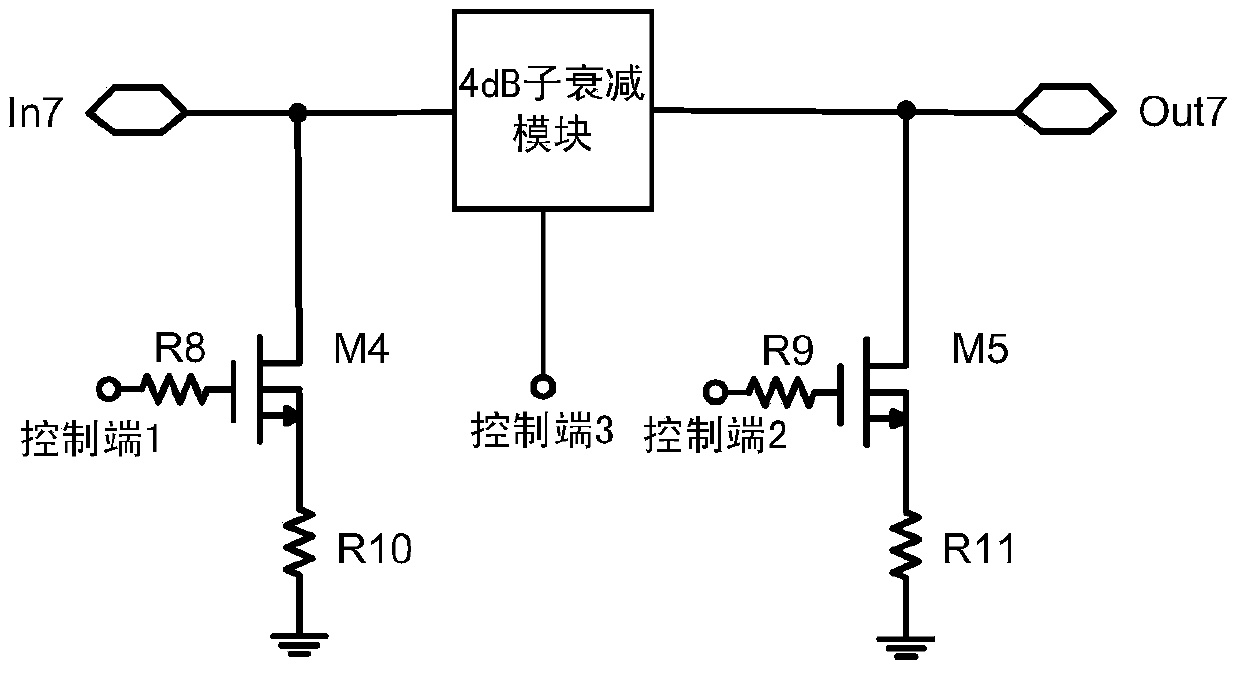
[0042] Embodiment 3: the working process of the 0~7dB combined attenuation mode of the present invention. Embodiment 3 of the present invention adopts Figure 6The MOS transistor switch shown serves as the control switch for the branch circuit, consisting of a Figure 4 The 4dB sub-attenuator module shown. The 0-7dB combined attenuation module is controlled by three digital signals at control terminal 1, control terminal 2 and control terminal 3 respectively. When the input of control terminal 1, control terminal 2, and control terminal 3 are all low level, the input of inverter Inv2 is low level, the output of inverter Inv2 is high level, switching MOS transistor M6 is turned on, and switching MOS transistor M4 , the switching MOS transistor M5 and the switching MOS transistor M7 are all turned off, and the 0-7dB combined attenuation module is in a reference state. When the input of control terminal 1 is high level, and the input of control terminal 2 and control terminal ...


PUM


Abstract

A low-differential-loss low-phase-shift high-integration-level five-level marching type ultra-wide-band numerical control attenuator is formed by a single signal channel which comprises a transmission line TL0, an 8dB attenuation module of a pai-type structure, an inductor L1, a 0-7dB combined attenuation module of a T type-bridge T type combined structure, an inductor L2, a 16dB attenuation module of a pai-type structure and a transmission TL1 in a cascaded mode in sequence based on the RF CMOS technology. An MOS tube is used as a control switch, five independent control ends controls three attenuation modules to work, an inducting network is used for phase compensation, working frequency range is Ku wave band within the attenuation range of 0-31 dB with marching length of 1dB, and 32-state low-differential-loss low-phase-shift signal amplitude attenuation can be achieved. The attenuator has the advantages of being low in differential loss, low in additional phase shift, low in production cost, small in chip area and compatible with a digital processing module, and the attenuator can be used for single-chip ultra-wide-band communication system integration.

Description

technical field [0001] The invention belongs to the technical field of communication, and further relates to a five-bit stepping ultra-wideband numerical control attenuator with low differential loss, low phase shift and high integration in the technical field of radar, communication and guidance electronic components. The invention can be used for the attenuation function of low differential loss and low phase shift realized by signal amplitude in ultra-wideband communication systems, radio frequency radio systems, military communication systems, phased array systems, and space communication transceiver systems. Background technique [0002] At present, in the technical fields of radar, communication, and guidance electronic components, ultra-wideband numerical control attenuators are widely used in ultra-wideband communication systems, radio frequency radio systems, military communication systems, phased array systems, and space communication transceiver systems. The numer...

Claims


Application Information

Patent Timeline
Patent Type & Authority Applications(China)
IPC IPC(8): H03H17/00
Inventor 庄奕琪李振荣张岩龙靳刚汤华莲张丽李聪曾志斌
Owner XIDIAN UNIV
Why Eureka
Try Eureka