

Three-dimensional multi-chip laminated module and manufacturing method thereof
A multi-chip module and chip technology, applied in semiconductor/solid-state device manufacturing, electrical components, electrical solid-state devices, etc., can solve the problems of chip processing and process yield reduction and high cost
- Summary
- Abstract
- Description
- Claims
- Application Information
AI Technical Summary
Problems solved by technology
Method used
Image

Examples
Embodiment Construction
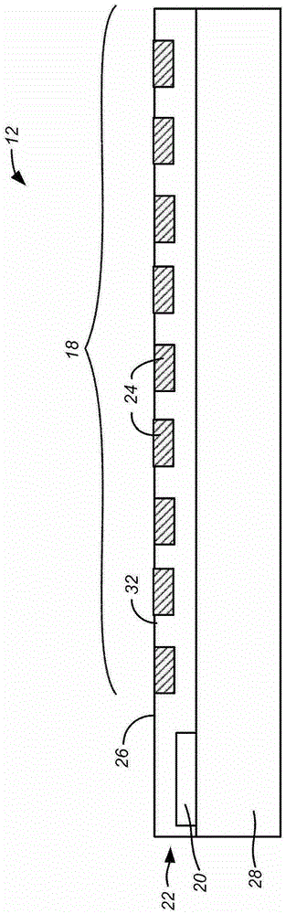
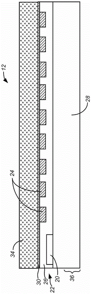
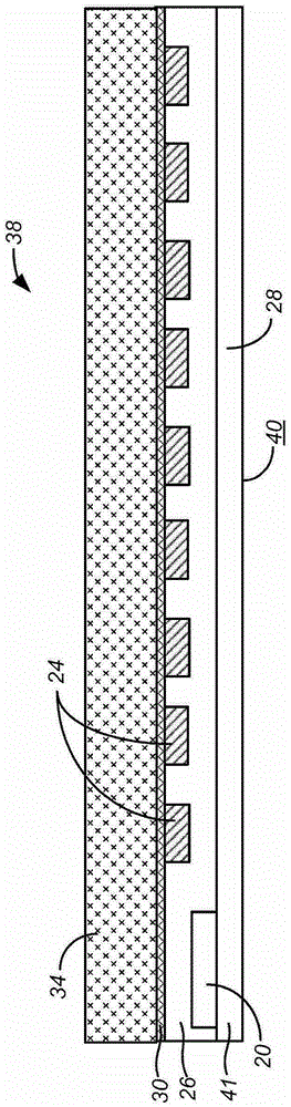
[0062] The present invention can be implemented in wafer scale stacking or diescale stacking. exist Figure 1-Figure 21 , the invention will be described in detail in terms of chip-level stacking. The advantages obtained by implementing the present invention using wafer-level stacking will be Figure 22-Figure 25 detail. Like elements in a wafer or chip will be denoted with like reference numerals.
[0063] figure 1 Is a simplified enlarged cross-sectional view of an IC chip 12 suitable for building a three-dimensional stacked multi-chip module in the manner described below. figure 1 The illustrated chip 12 includes an electrical contact area 18 and an active device circuit 20 , both within a patterned conductive layer 22 . The patterned conductive layer 22 includes a dielectric layer 26 overlying and supported by a substrate 28 of the chip 12 . Substrate 28 is typically silicon. The electrical contact area 18 includes a plurality of electrical conductors 24, typically ...
PUM
 Abstract
Description
Claims
Application Information