

One-dimensional tin selenide nanoarray as well as preparation method and application thereof
A nano-array, tin selenide technology, applied in the direction of nanotechnology, binary selenium/tellurium compound, gaseous chemical plating, etc., can solve the problem of no discovery
- Summary
- Abstract
- Description
- Claims
- Application Information
AI Technical Summary
Problems solved by technology
Method used
Image

Examples
Embodiment 1
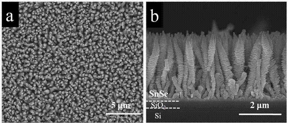
[0074] Example 1 Preparation of one-dimensional tin selenide nanoarrays by chemical vapor deposition
[0075] (1) Mix 5g of high-purity (purity 99.999%) SnSe powder and 0.2g of bismuth powder (purity 99.99%) thoroughly, grind them in a mortar for 40min, and use them as growth evaporation sources;
[0076] (2) Place the silicon wafer in a mixed solution of 21mL of concentrated sulfuric acid and 7mL of hydrogen peroxide, heat it to 130°C, and clean the surface of the silicon wafer for 2 hours; then ultrasonicate the silicon wafer with deionized water and dry it with nitrogen gas to serve as the substrate of the silicon wafer;
[0077] (3) Take 0.1 g of the powder prepared in step (1) and place it in the central temperature zone of a tube reactor (OTF-1200X (single temperature zone) open vacuum tube furnace, Hefei Kejing, Anhui) as an evaporation source , and place the growth substrate 30cm below the airflow;
[0078] (4) Pass 35sccm argon gas into the tube reactor, and clean it...
Embodiment 2
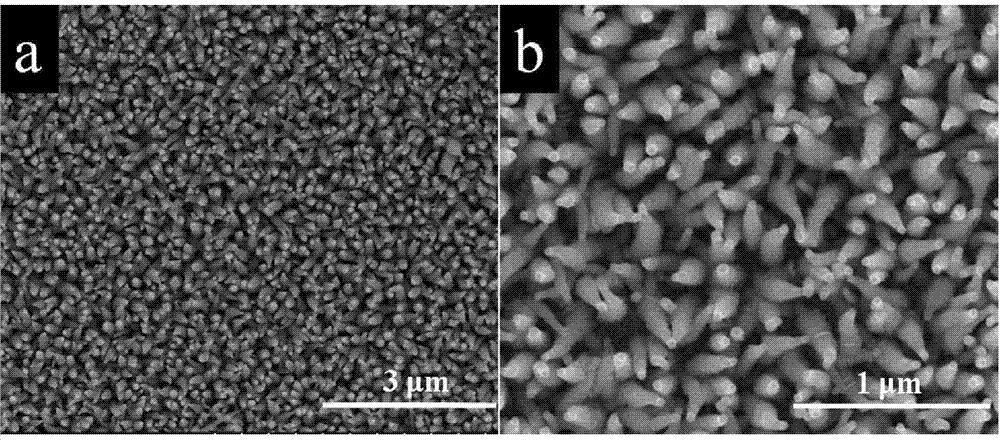
[0084] Example 2 Preparation of one-dimensional tin selenide nanoarrays by chemical vapor deposition
[0085] (1) Fully mix 5g of high-purity (purity 99.8%) SnSe powder and 0.2g of bismuth powder (purity 99.9%), and grind them in a mortar for 60 minutes as a growth evaporation source;
[0086] (2) Place the silicon wafer in a mixed solution of 21mL of concentrated sulfuric acid and 7mL of hydrogen peroxide, heat it to 130°C, and clean the surface of the silicon wafer for 2h; then ultrasonicate the silicon wafer with deionized water and blow it dry with nitrogen, as a growing silicon wafer base;
[0087] (3) Take 0.1 g of the powder prepared in step (1) and place it in the central temperature zone of a tube reactor (OTF-1200X (single temperature zone) open vacuum tube furnace, Hefei Kejing, Anhui) as an evaporation source material, and place the growth substrate 31 cm below its airflow;
[0088] (4) Pass 35sccm argon gas into the tube reactor, and clean it three times continu...
Embodiment 3
[0091] Example 3 Preparation of one-dimensional tin selenide nanoarrays by chemical vapor deposition
[0092] (1) Fully mix 5g of high-purity (purity 99.8%) SnSe powder and 0.2g of bismuth powder (purity 99.9%), and grind them in a mortar for 40min as a growth evaporation source;
[0093] (2) Place the silicon wafer in a mixed solution of 21mL of concentrated sulfuric acid and 7mL of hydrogen peroxide, heat it to 130°C, and clean the surface of the silicon wafer for 2h; then ultrasonicate the silicon wafer with deionized water and blow it dry with nitrogen, as a growing silicon wafer base;
[0094] (3) Take 0.1 g of the powder prepared in step (1) and place it in the central temperature zone of a tube reactor (OTF-1200X (single temperature zone) open vacuum tube furnace, Hefei Kejing, Anhui) as an evaporation source material, and place the growth substrate 30 cm below its airflow;
[0095] (4) Pass 35sccm argon gas into the tube reactor, and clean it three times continuously...
PUM
| Property | Measurement | Unit |
|---|---|---|
| Diameter | aaaaa | aaaaa |
| Diameter | aaaaa | aaaaa |
Abstract
Description
Claims
Application Information