Super-hard semiconductor material polishing method

A semiconductor and superhard technology, which is applied in semiconductor/solid-state device manufacturing, grinding/polishing equipment, surface polishing machine tools, etc., can solve problems such as scratches, achieve high flatness, reduce costs, and increase yield.

Active Publication Date: 2014-01-15
安徽微芯长江半导体材料有限公司
View PDF7 Cites 21 Cited by
  • Summary
  • Abstract
  • Description
  • Claims
  • Application Information

AI Technical Summary

Problems solved by technology

[0008] In addition, traditional superhard semiconductor materials (such as SiC, Al 2 o 3 ) Polishing technology, on the one hand, is completely different for different materials, such as SiC and Al 2 o 3 The polishing process is completely different. Using these two different polishing processes on the same equipment at the same time may have a great impact on the machine and polishing efficiency.
This increases a lot of difficulties for a department that completes the processing of these two crystal materials at the same time; on the other hand, the traditional process does not match the rough polishing, fine polishing and chemical mechanical polishing processes well, making Superhard semiconductor materials (such as SiC, Al 2 o 3 ) surface still has scratches and subsurface damaged layers

Method used


Image

  • Super-hard semiconductor material polishing method
  • Super-hard semiconductor material polishing method
  • Super-hard semiconductor material polishing method

Examples


Embodiment 1

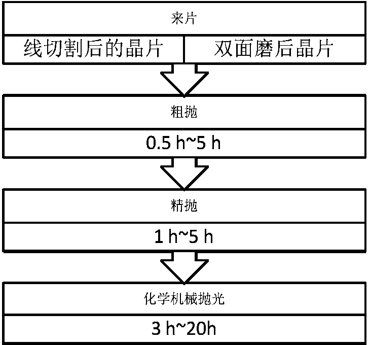
[0032] The ultra-hard semiconductor material SiC wafer with a thickness of 450 ± 10 μm, a line mark depth of less than 10 μm, a warpage of less than 50 μm, and a thickness non-uniformity of less than 30 μm after wire cutting is polished using the process described in the present invention: first, use The diamond polishing liquid with a pH value of 7.0, a concentration of 20%, and a particle size of 5 μm uses a polishing cloth with a Shore hardness of 70, and the polishing pressure is controlled at 5 g / cm 2 , the rotational speed of the polishing disc is 80 rpm, and rough polishing is performed for 5 hours. Then use a diamond polishing liquid with a pH value of 7.0, a concentration of 20%, and a particle size of 2 μm, using a polishing cloth with a Shore hardness of 60, and controlling the polishing pressure to 5 g / cm 2 , the rotational speed of the polishing disc is 70rpm, and the fine polishing is carried out for 5h. Then, the silica sol with a pH value of 9.5, a concentrati...

Embodiment 2

[0034] For wire-cut superhard semiconductor material Al with a thickness of 450±10 μm, a line trace depth of less than 10 μm, a warpage of less than 50 μm, and a thickness unevenness of less than 30 μm 2 o 3 The wafer is polished by the process described in the present invention: first, the diamond polishing liquid with a pH value of 7.0, a concentration of 20%, and a particle diameter of 5 μm is used, and a polishing cloth with a Shore hardness of 70 is used, and the controlled polishing pressure is 5 g / cm 2 , the rotational speed of the polishing disc is 80 rpm, and rough polishing is performed for 5 hours. Then use a diamond polishing liquid with a pH value of 7.0, a concentration of 20%, and a particle size of 2 μm, using a polishing cloth with a Shore hardness of 60, and controlling the polishing pressure to 5 g / cm 2 , the rotational speed of the polishing disc is 70rpm, and the fine polishing is carried out for 5h. Then, the silica sol with a pH value of 9.5, a concent...

Embodiment 3

[0036] The ultra-hard semiconductor material SiC wafer with a thickness of 450 ± 10 μm, a line mark depth of less than 10 μm, a warpage of less than 50 μm, and a thickness non-uniformity of less than 30 μm after wire cutting is polished using the process described in the present invention: first, use The diamond polishing liquid with a pH value of 3.0, a concentration of 3%, and a particle size of 1.5 μm uses a polishing cloth with a Shore hardness of 70, and the polishing pressure is controlled at 2 g / cm 2 , the rotational speed of the polishing disc was 30 rpm, and rough polishing was performed for 7 hours. Then use a diamond polishing liquid with a pH value of 7.0, a concentration of 20%, and a particle size of 2 μm, using a polishing cloth with a Shore hardness of 60, and controlling the polishing pressure to 5 g / cm 2 , the rotational speed of the polishing disc is 70rpm, and the fine polishing is carried out for 5h. Then, the silica sol with a pH value of 9.5, a concentr...


PUM

PropertyMeasurementUnit
particle diameteraaaaaaaaaa

Abstract

The invention relates to a super-hard semiconductor material polishing method. According to the method, a machined super-hard semiconductor material can be extremely low in surface roughness and have an atomic stepped surface through three polishing process flows with very approximate parameters, including rough polishing, fine polishing and chemico-mechanical polishing. Due to the fact that only the three processes are used, the method simplifies the super-hard material polishing flows greatly, lowers cost, guarantees the consistency and stability of machining quality and improves the rate of finished products.

Description

technical field [0001] The invention relates to the field of semiconductor material processing and device preparation, in particular to a superhard semiconductor material polishing method, in particular to a superhard semiconductor material (such as SiC, Al2O3) polishing method capable of obtaining atomic step surfaces. Background technique [0002] Alumina (Al 2 o 3 ), silicon carbide (SiC), aluminum nitride (AlN) and gallium nitride (GaN) and other superhard semiconductor materials are important representatives of wide bandgap semiconductors. High thermal conductivity, high electron saturation drift speed, strong radiation resistance and good chemical stability, etc., have become the key semiconductor materials for manufacturing new generation of microelectronic devices and circuits after silicon, germanium and gallium arsenide. al 2 o 3 , SiC, AlN, etc. have unique advantages in the production of high-power microwave devices, high-temperature and radiation-resistant d...

Claims


Application Information

Patent Timeline
Patent Type & Authority Applications(China)
IPC IPC(8): B24B29/02H01L21/304C09G1/02
CPCB24B1/00C09G1/02H01L21/304
Inventor 黄维王乐星庄击勇陈辉杨建华施尔畏
Owner 安徽微芯长江半导体材料有限公司
Why Eureka
Try Eureka